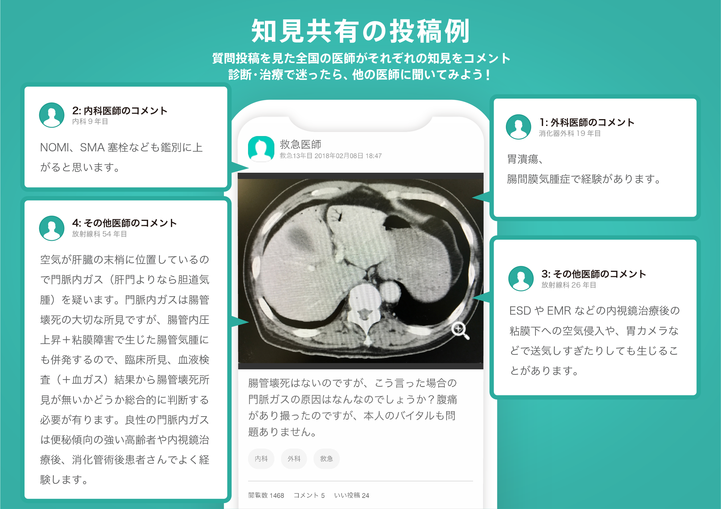
著名医師による解説が無料で読めます
すると翻訳の精度が向上します
最近、多層ソフトリソグラフィーを使用してエラストマーを型にすることにより、数百の独立したバルブを備えた洗練された流体回路が構築されました。ただし、このマイクロ流体回路の縮小は、回路を制御する作動とインターフェース要素の対応する小型化とは一致していません。流体回路は小さい(幅約10〜100ミクロンのチャネル)が、外部の空気圧ソレノイドとチューブまたは各独立したバルブを制御する機械的ピンで構成されるメデューサの頭のような界面は、1〜4桁大きくなっています(およそmmからcm)。その結果、ポータブルで高スループットアプリケーションのためにマイクロ流体に大規模な統合を使用するという夢は阻害されています。多層ソフトリソグラフィと形状記憶合金(SMA)を組み合わせることにより、印刷回路板(PCB)に組み立てられるバルブ、ポンプ、ラッチ、マルチプレクサなどの電子的に活性化されたマイクロ流体成分を示します。したがって、高密度、電子制御されたマイクロ流体チップは、PCB上の標準光電子成分とともに統合できます。さらに、バルブ状態の組み合わせであるマイクロ流体状態のアイデアを紹介し、積分回路(IC)マイクロプロセッサの命令セットに類似しています。マイクロ流体状態は、ハードウェアまたはソフトウェアで表される場合があり、外部制御ラインの対数削減をもたらす制御アーキテクチャを提案します。これらの開発により、物理的にも抽象的なモデルの両方に似た電子ICに似たマイクロ流体回路の構築に近づきます。
最近、多層ソフトリソグラフィーを使用してエラストマーを型にすることにより、数百の独立したバルブを備えた洗練された流体回路が構築されました。ただし、このマイクロ流体回路の縮小は、回路を制御する作動とインターフェース要素の対応する小型化とは一致していません。流体回路は小さい(幅約10〜100ミクロンのチャネル)が、外部の空気圧ソレノイドとチューブまたは各独立したバルブを制御する機械的ピンで構成されるメデューサの頭のような界面は、1〜4桁大きくなっています(およそmmからcm)。その結果、ポータブルで高スループットアプリケーションのためにマイクロ流体に大規模な統合を使用するという夢は阻害されています。多層ソフトリソグラフィと形状記憶合金(SMA)を組み合わせることにより、印刷回路板(PCB)に組み立てられるバルブ、ポンプ、ラッチ、マルチプレクサなどの電子的に活性化されたマイクロ流体成分を示します。したがって、高密度、電子制御されたマイクロ流体チップは、PCB上の標準光電子成分とともに統合できます。さらに、バルブ状態の組み合わせであるマイクロ流体状態のアイデアを紹介し、積分回路(IC)マイクロプロセッサの命令セットに類似しています。マイクロ流体状態は、ハードウェアまたはソフトウェアで表される場合があり、外部制御ラインの対数削減をもたらす制御アーキテクチャを提案します。これらの開発により、物理的にも抽象的なモデルの両方に似た電子ICに似たマイクロ流体回路の構築に近づきます。
Recently, sophisticated fluidic circuits with hundreds of independent valves have been built by using multi-layer soft-lithography to mold elastomers. However, this shrinking of microfluidic circuits has not been matched by a corresponding miniaturization of the actuation and interfacing elements that control the circuits; while the fluidic circuits are small ( approximately 10-100 micron wide channels), the Medusa's head-like interface, consisting of external pneumatic solenoids and tubing or mechanical pins to control each independent valve, is larger by one to four orders of magnitude (approximately mm to cm). Consequently, the dream of using large scale integration in microfluidics for portable, high throughput applications has been stymied. By combining multi-layer soft-lithography with shape memory alloys (SMA), we demonstrate electronically activated microfluidic components such as valves, pumps, latches and multiplexers, that are assembled on printed circuit boards (PCBs). Thus, high density, electronically controlled microfluidic chips can be integrated alongside standard opto-electronic components on a PCB. Furthermore, we introduce the idea of microfluidic states, which are combinations of valve states, and analogous to instruction sets of integrated circuit (IC) microprocessors. Microfluidic states may be represented in hardware or software, and we propose a control architecture that results in logarithmic reduction of external control lines. These developments bring us closer to building microfluidic circuits that resemble electronic ICs both physically, as well as in their abstract model.
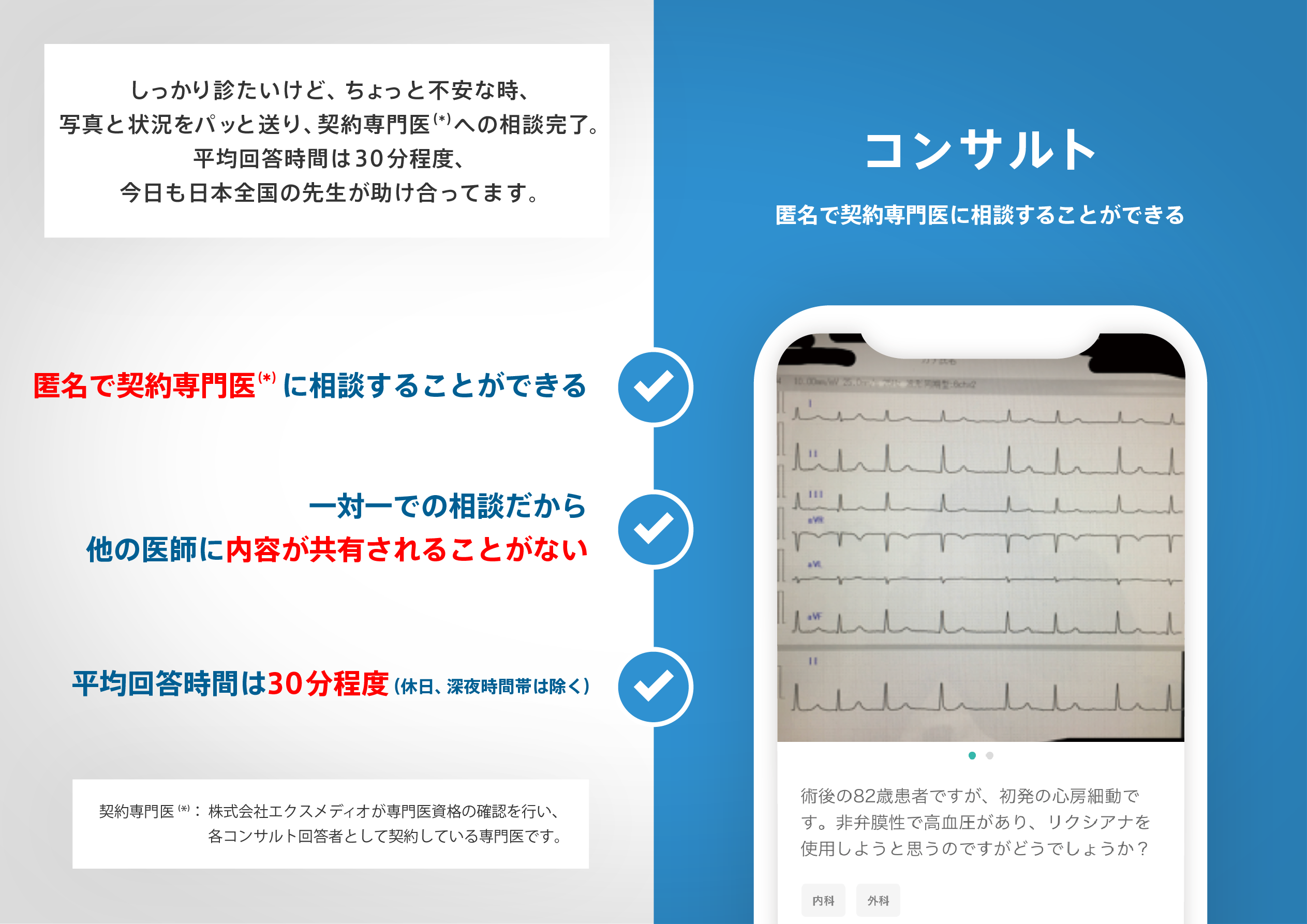
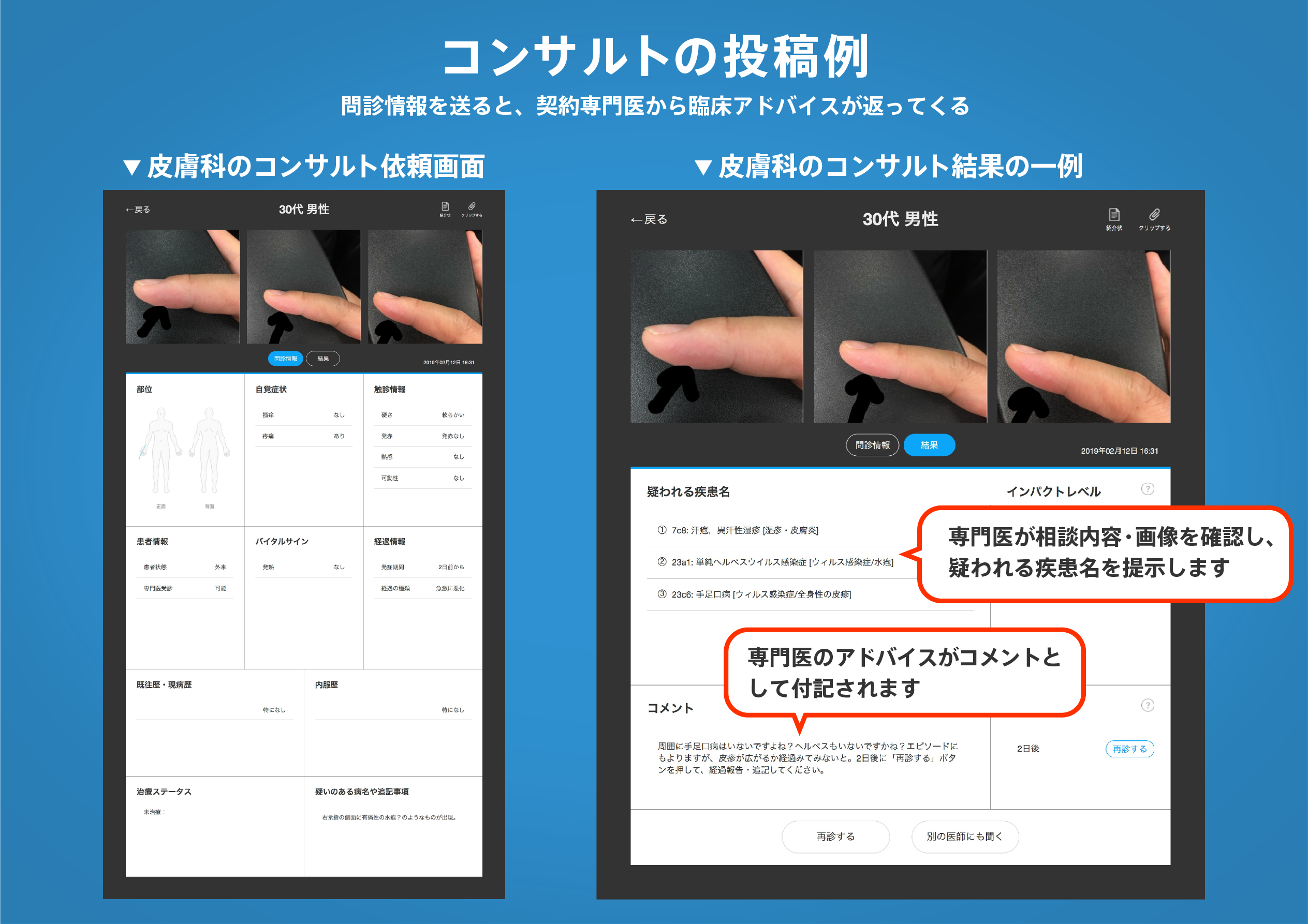
医師のための臨床サポートサービス
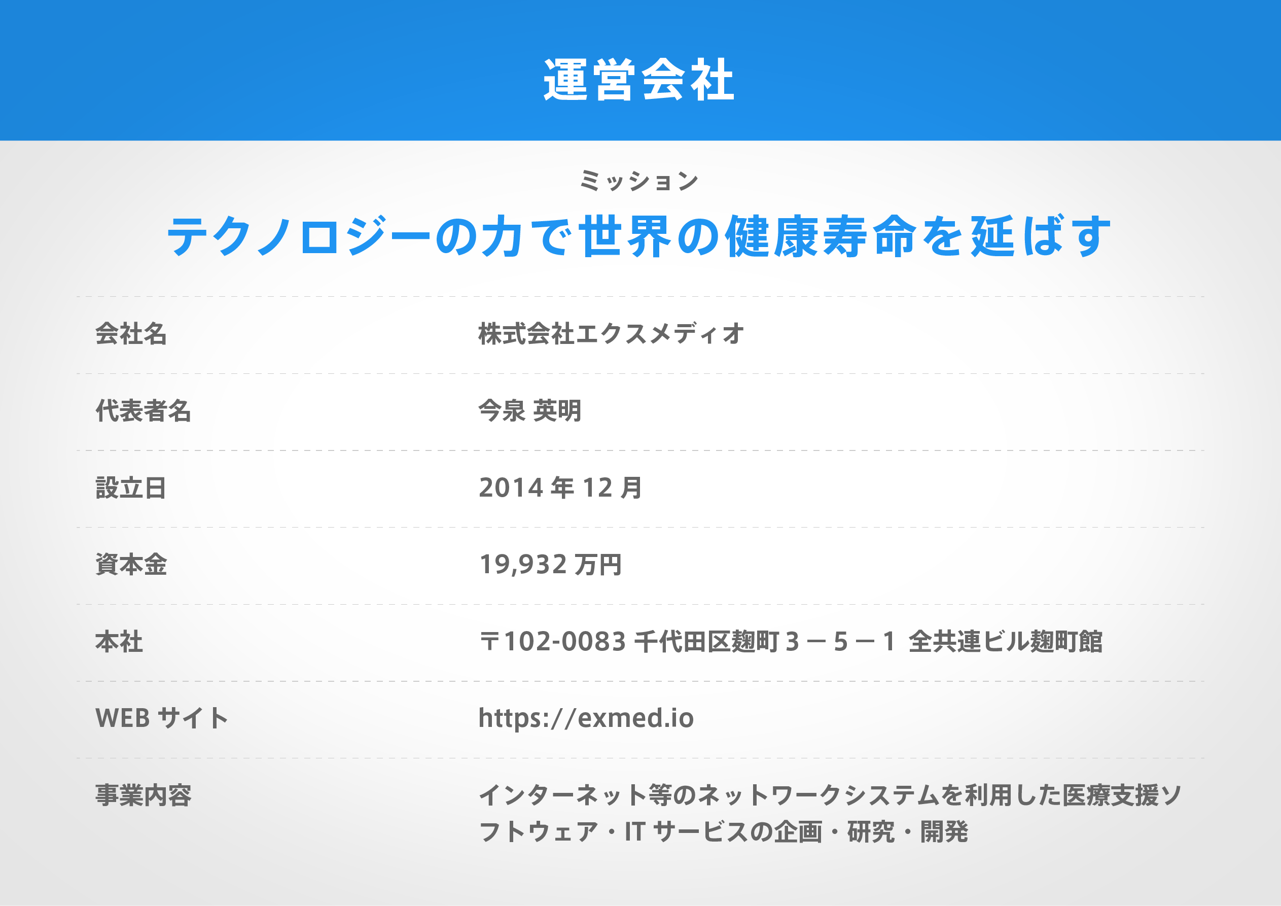
ヒポクラ x マイナビのご紹介


無料会員登録していただくと、さらに便利で効率的な検索が可能になります。