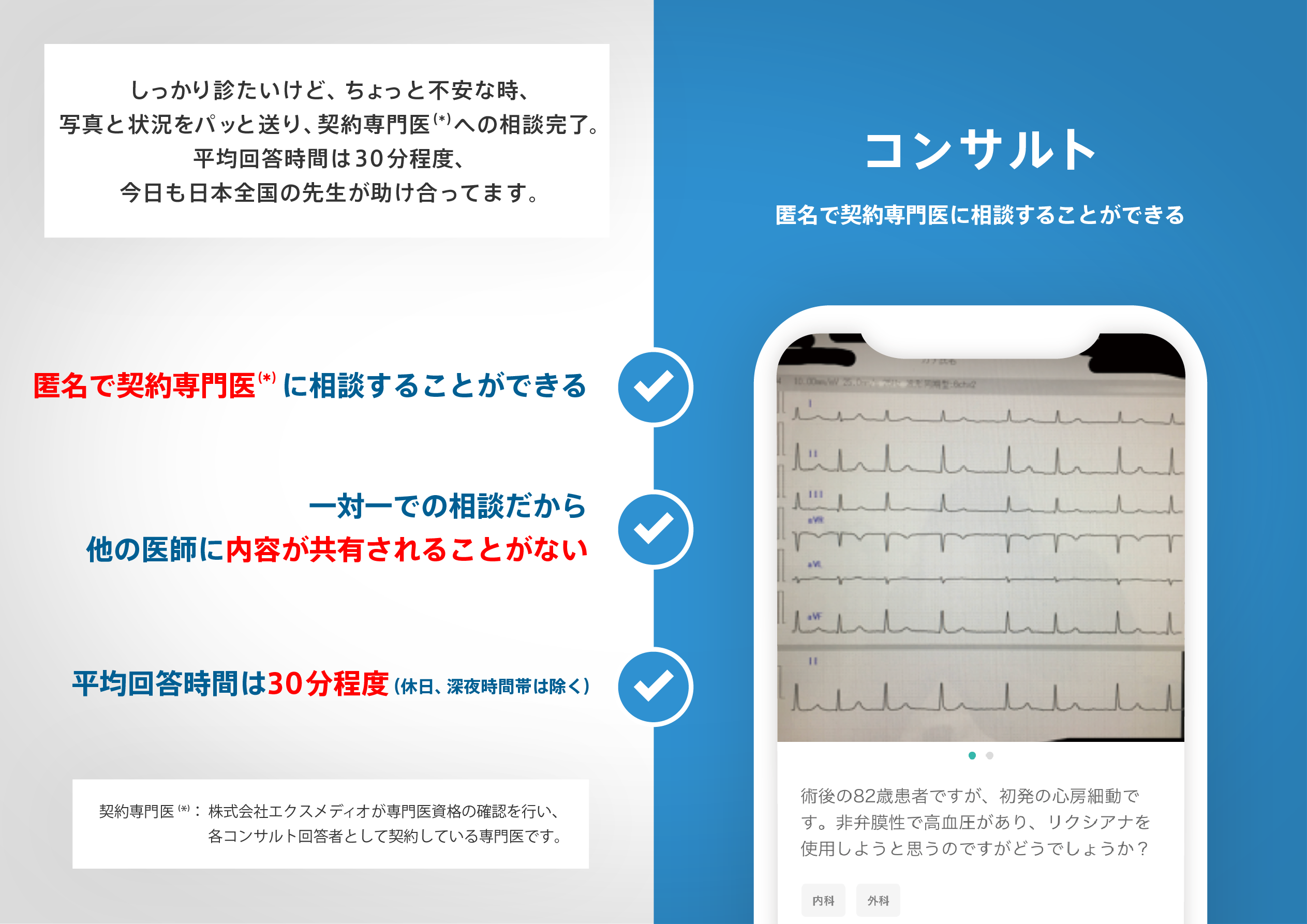
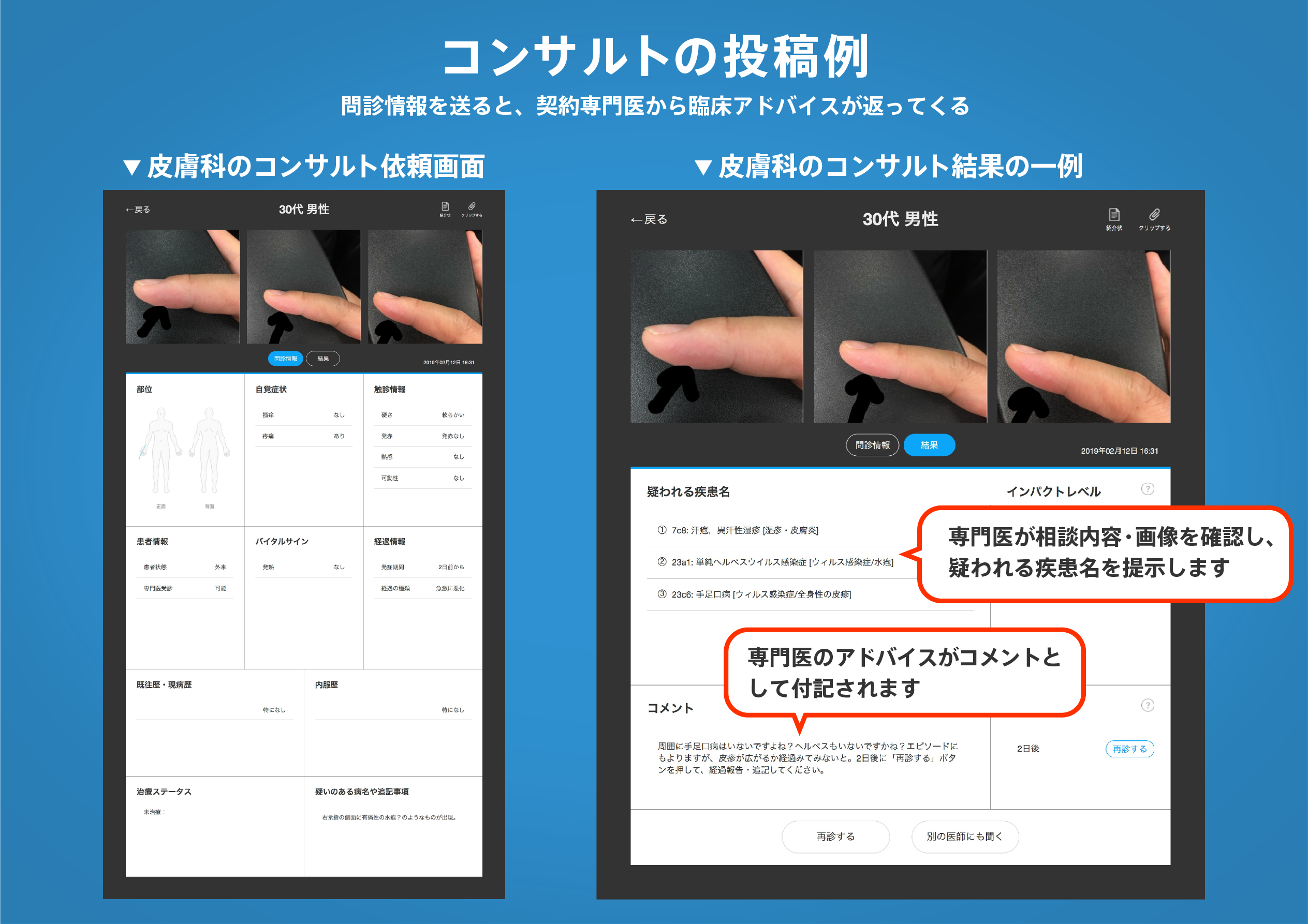
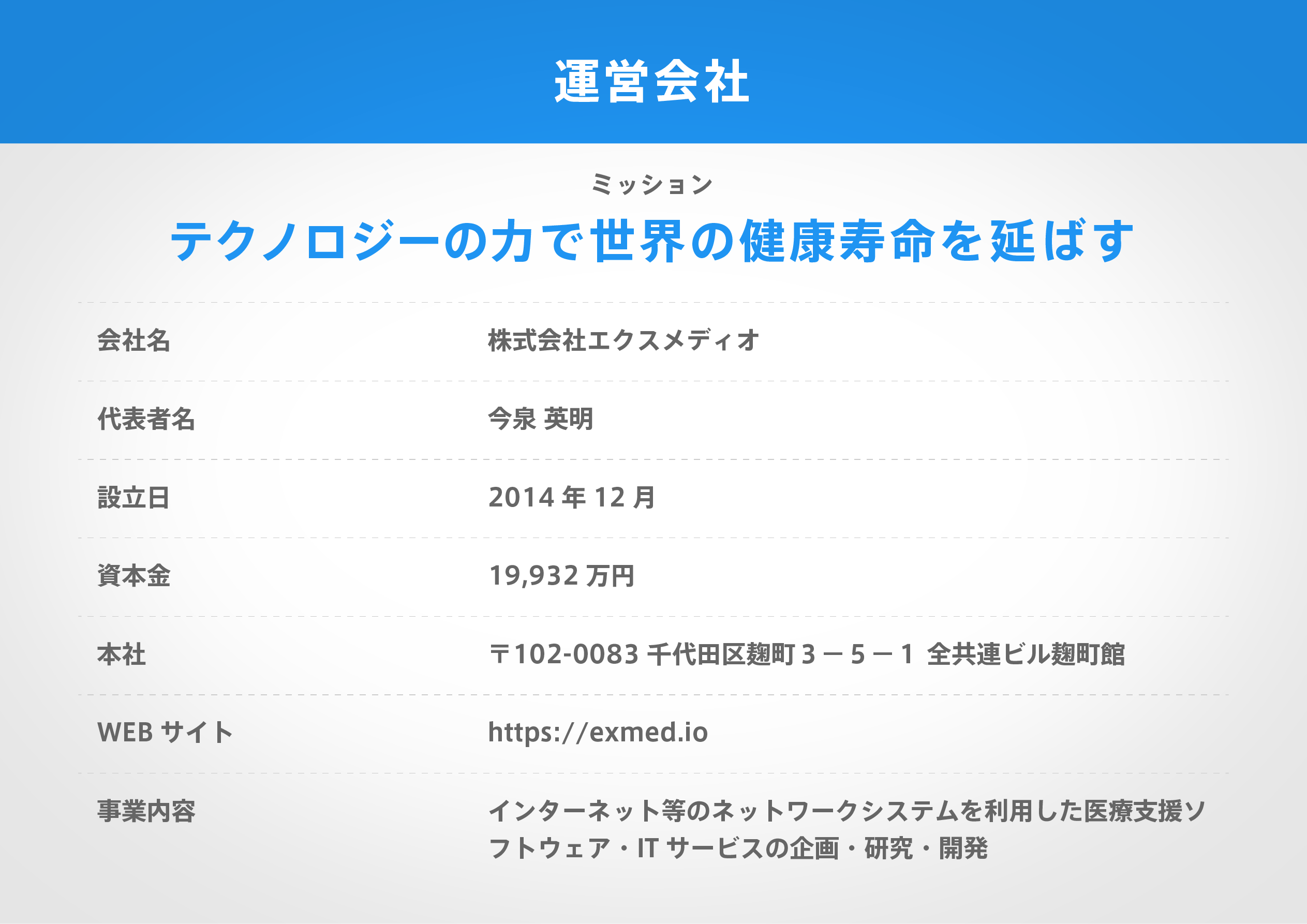
著名医師による解説が無料で読めます
すると翻訳の精度が向上します
III-V半導体ナノ膜の調整可能な表面形態は、半導体の電子構造と光相互作用を調節する機会を提供します。ここでは、PDMSマイクロウェルアレイ上のインガアスナノメンブレン(厚さ、42 nm)の秩序あるしわの形成のための真空誘導したしわ方法を導入し、半導体ナノメンブレーンの決定論的および多方向しわエンジニアリングの戦略として紹介します。このアプローチでは、ナノ膜で覆われたマイクロウェルパターンの外側と内側の内側の真空誘起圧力差は、事前に定義されたマイクロウェルでナノ膜の膨らみにつながり、これにより、ナノ膜の間のナノ膜のストレッチ誘導のしわ形成が生じます。マイクロウェル。ナノメンブレンのしわの方向とジオメトリは、マイクロウェルのPDMモジュラス、深さ、形状、およびナノメンブレンの不均一基質への移動印刷中の温度を変化させることにより、適切に制御されています。ここに示されているしわの方法は、他の半導体ナノ膜に適用でき、調整可能な電子プロパティを備えた型破りな電子デバイスを実現するための重要なプラットフォームを作成することができます。
III-V半導体ナノ膜の調整可能な表面形態は、半導体の電子構造と光相互作用を調節する機会を提供します。ここでは、PDMSマイクロウェルアレイ上のインガアスナノメンブレン(厚さ、42 nm)の秩序あるしわの形成のための真空誘導したしわ方法を導入し、半導体ナノメンブレーンの決定論的および多方向しわエンジニアリングの戦略として紹介します。このアプローチでは、ナノ膜で覆われたマイクロウェルパターンの外側と内側の内側の真空誘起圧力差は、事前に定義されたマイクロウェルでナノ膜の膨らみにつながり、これにより、ナノ膜の間のナノ膜のストレッチ誘導のしわ形成が生じます。マイクロウェル。ナノメンブレンのしわの方向とジオメトリは、マイクロウェルのPDMモジュラス、深さ、形状、およびナノメンブレンの不均一基質への移動印刷中の温度を変化させることにより、適切に制御されています。ここに示されているしわの方法は、他の半導体ナノ膜に適用でき、調整可能な電子プロパティを備えた型破りな電子デバイスを実現するための重要なプラットフォームを作成することができます。
Tunable surface morphology in III-V semiconductor nanomembranes provides opportunities to modulate electronic structures and light interactions of semiconductors. Here, we introduce a vacuum-induced wrinkling method for the formation of ordered wrinkles in InGaAs nanomembranes (thickness, 42 nm) on PDMS microwell arrays as a strategy for deterministic and multidirectional wrinkle engineering of semiconductor nanomembranes. In this approach, a vacuum-induced pressure difference between the outer and inner sides of the microwell patterns covered with nanomembranes leads to bulging of the nanomembranes at the predefined microwells, which, in turn, results in stretch-induced wrinkle formation of the nanomembranes between the microwells. The direction and geometry of the nanomembrane wrinkles are well controlled by varying the PDMS modulus, depth, and shape of microwells, and the temperature during the transfer printing of nanomembrane onto heterogeneous substrates. The wrinkling method shown here can be applied to other semiconductor nanomembranes and may create an important platform to realize unconventional electronic devices with tunable electronic properties.
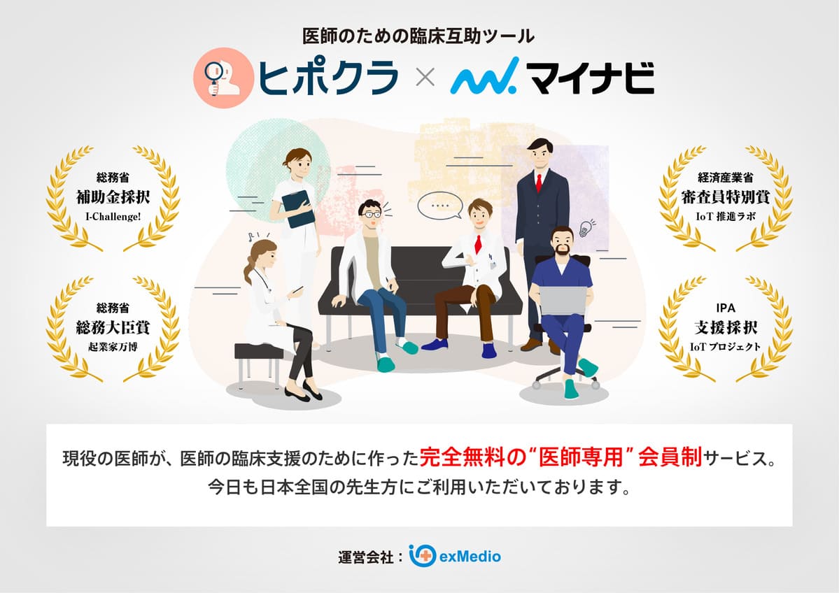
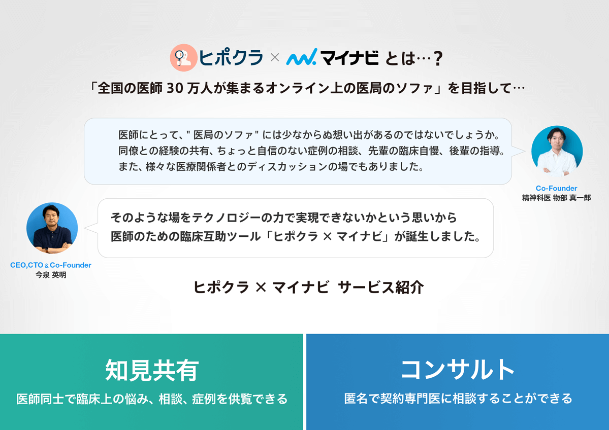
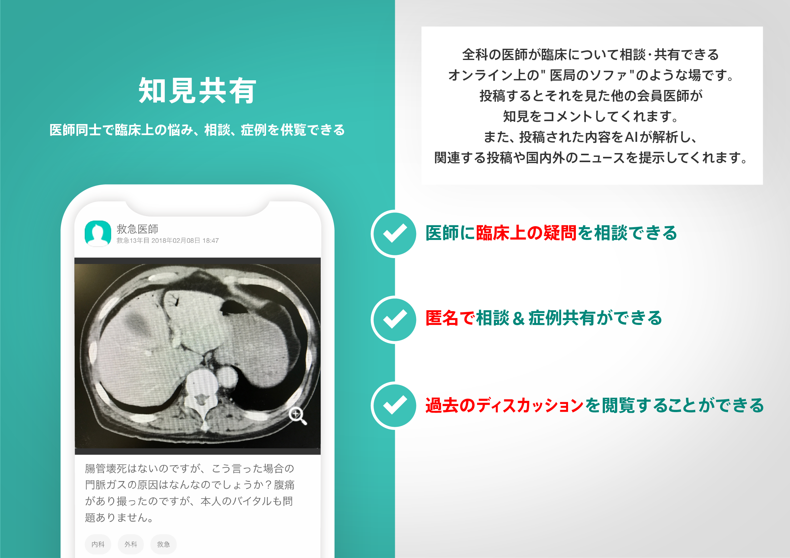
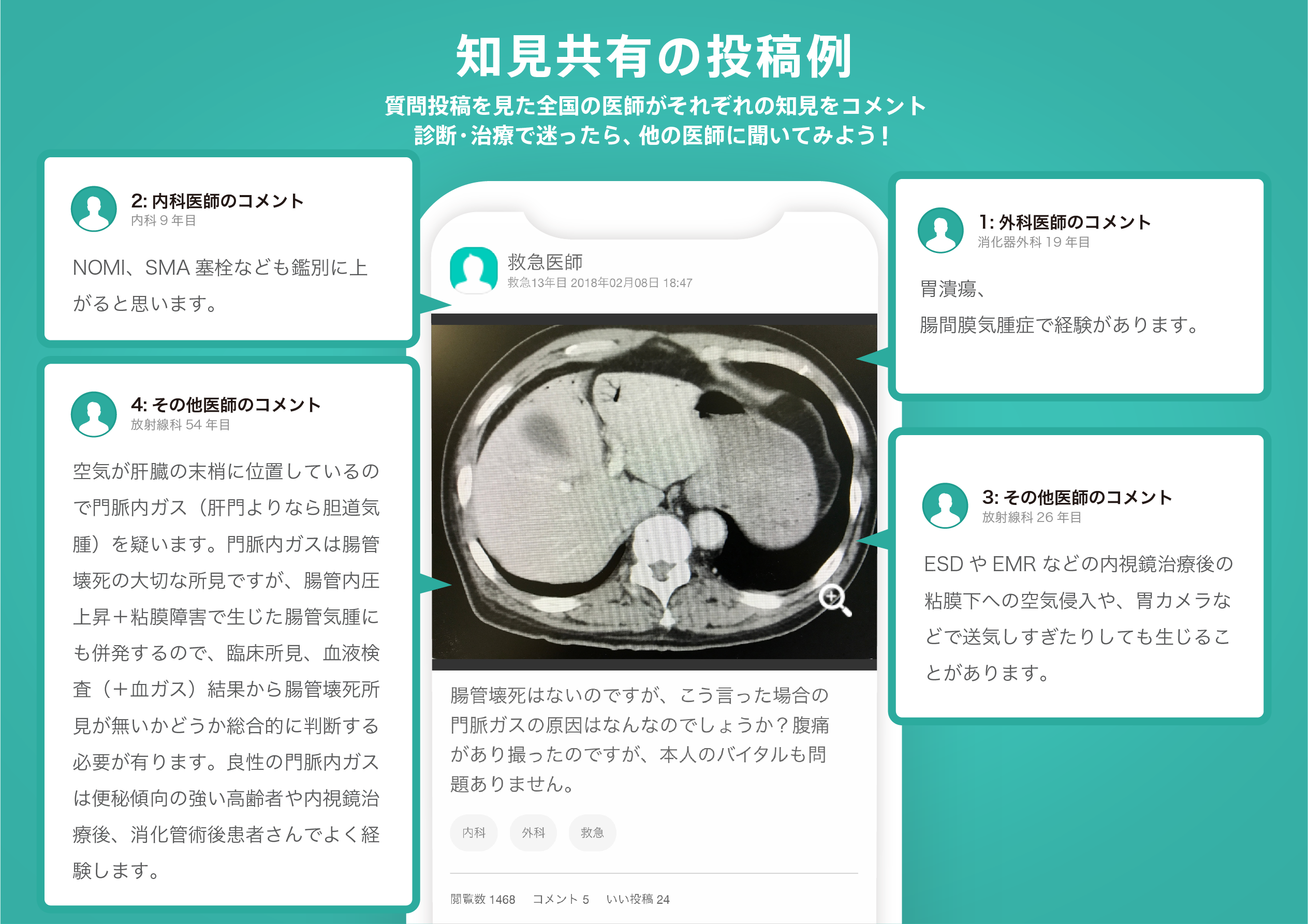
医師のための臨床サポートサービス
ヒポクラ x マイナビのご紹介
無料会員登録していただくと、さらに便利で効率的な検索が可能になります。