著名医師による解説が無料で読めます
すると翻訳の精度が向上します
半導体ナノ構造の制御された製造は、高性能フォトニックおよび光電子デバイスのエンジニアリングに不可欠なステップです。特に、ダイヤモンドは最近、量子技術、フォトニクス、高解像度センシングアプリケーションの有望なプラットフォームとしてかなりの注目を集めています。ここでは、ガスを介した電子ビーム誘導エッチング(EBIE)を使用した光学的に活性な機能的なダイヤモンド構造の製造を示します。この技術は、水蒸気環境でのエネルギー電子による表面吸着H2O分子の解離を通じて、室温で乾燥化学エッチングを実現します。電子洪水暴露とエッチングマスクの使用によって平行処理が可能ですが、ダイヤモンド微粒子の傾斜ファセットの直接書き込みエッチングによって高解像度のマスクのない反復編集が実証されます。実現された構造は、ダイヤモンド内の光学的に活性な構造の製造のためのEBIEの可能性を示しています。
半導体ナノ構造の制御された製造は、高性能フォトニックおよび光電子デバイスのエンジニアリングに不可欠なステップです。特に、ダイヤモンドは最近、量子技術、フォトニクス、高解像度センシングアプリケーションの有望なプラットフォームとしてかなりの注目を集めています。ここでは、ガスを介した電子ビーム誘導エッチング(EBIE)を使用した光学的に活性な機能的なダイヤモンド構造の製造を示します。この技術は、水蒸気環境でのエネルギー電子による表面吸着H2O分子の解離を通じて、室温で乾燥化学エッチングを実現します。電子洪水暴露とエッチングマスクの使用によって平行処理が可能ですが、ダイヤモンド微粒子の傾斜ファセットの直接書き込みエッチングによって高解像度のマスクのない反復編集が実証されます。実現された構造は、ダイヤモンド内の光学的に活性な構造の製造のためのEBIEの可能性を示しています。
Controlled fabrication of semiconductor nanostructures is an essential step in engineering of high performance photonic and optoelectronic devices. Diamond in particular has recently attracted considerable attention as a promising platform for quantum technologies, photonics and high resolution sensing applications. Here we demonstrate the fabrication of optically active, functional diamond structures using gas-mediated electron beam induced etching (EBIE). The technique achieves dry chemical etching at room temperature through the dissociation of surface-adsorbed H2O molecules by energetic electrons in a water vapor environment. Parallel processing is possible by electron flood exposure and the use of an etch mask, while high resolution, mask-free, iterative editing is demonstrated by direct write etching of inclined facets of diamond microparticles. The realized structures demonstrate the potential of EBIE for the fabrication of optically active structures in diamond.
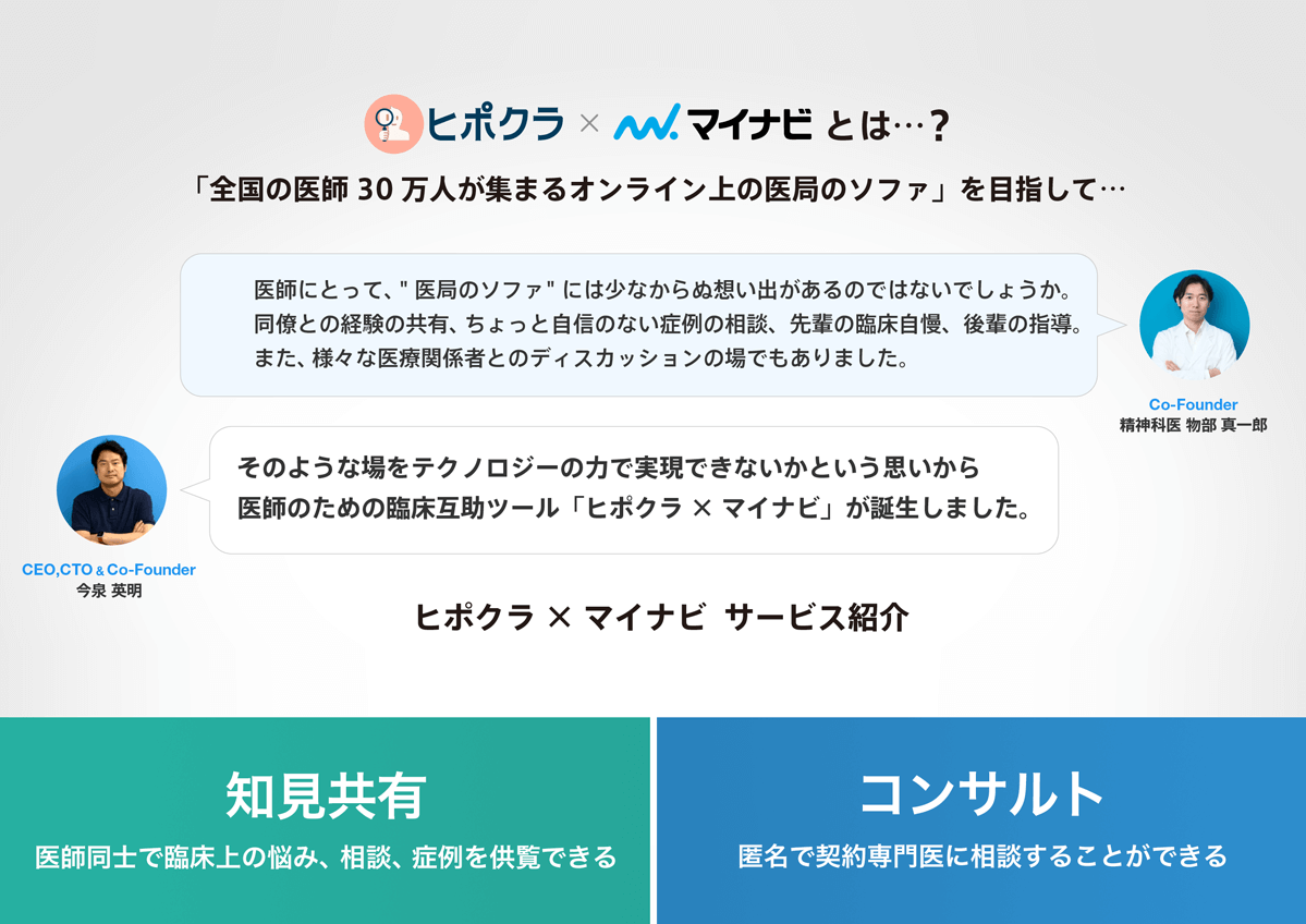
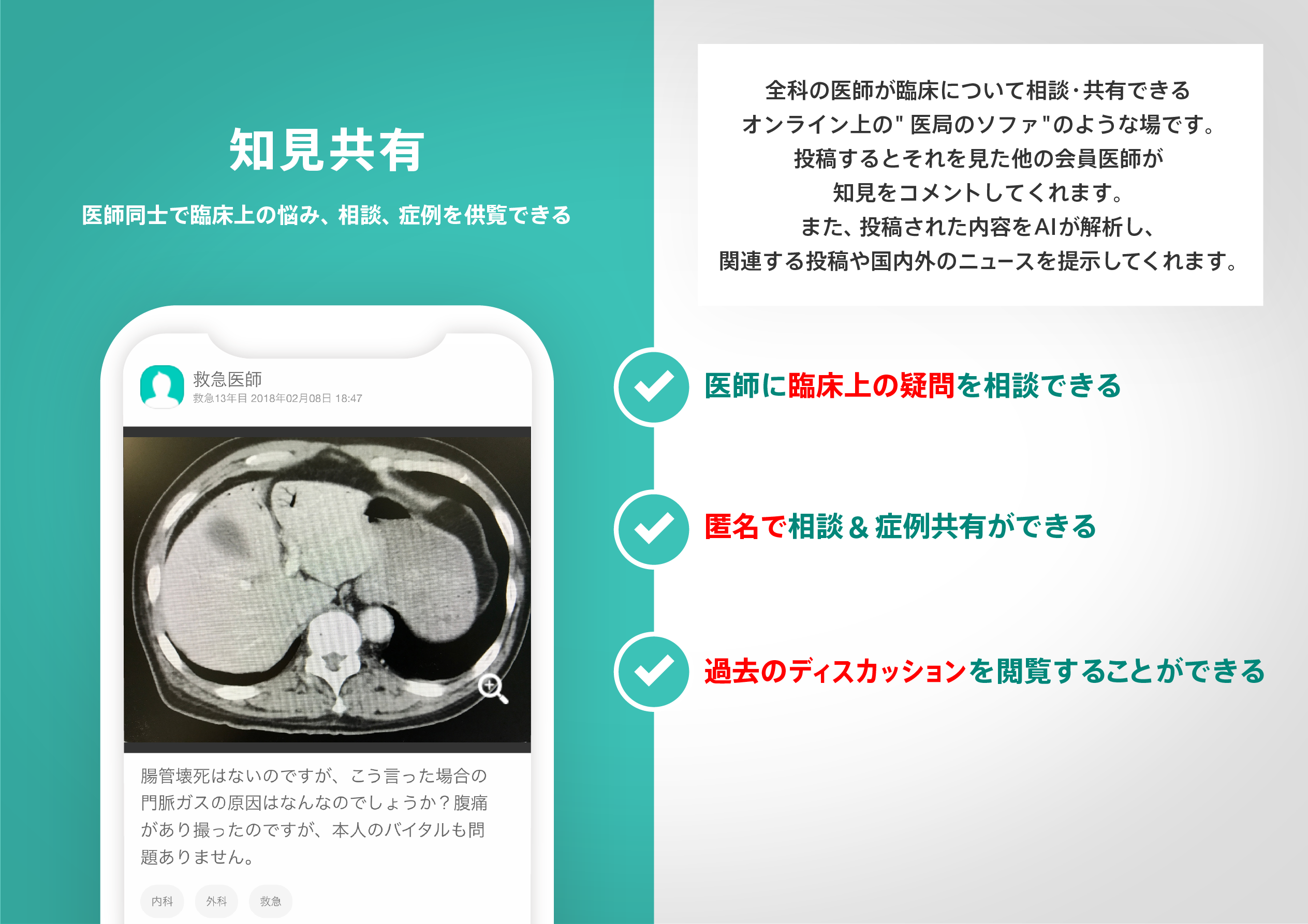
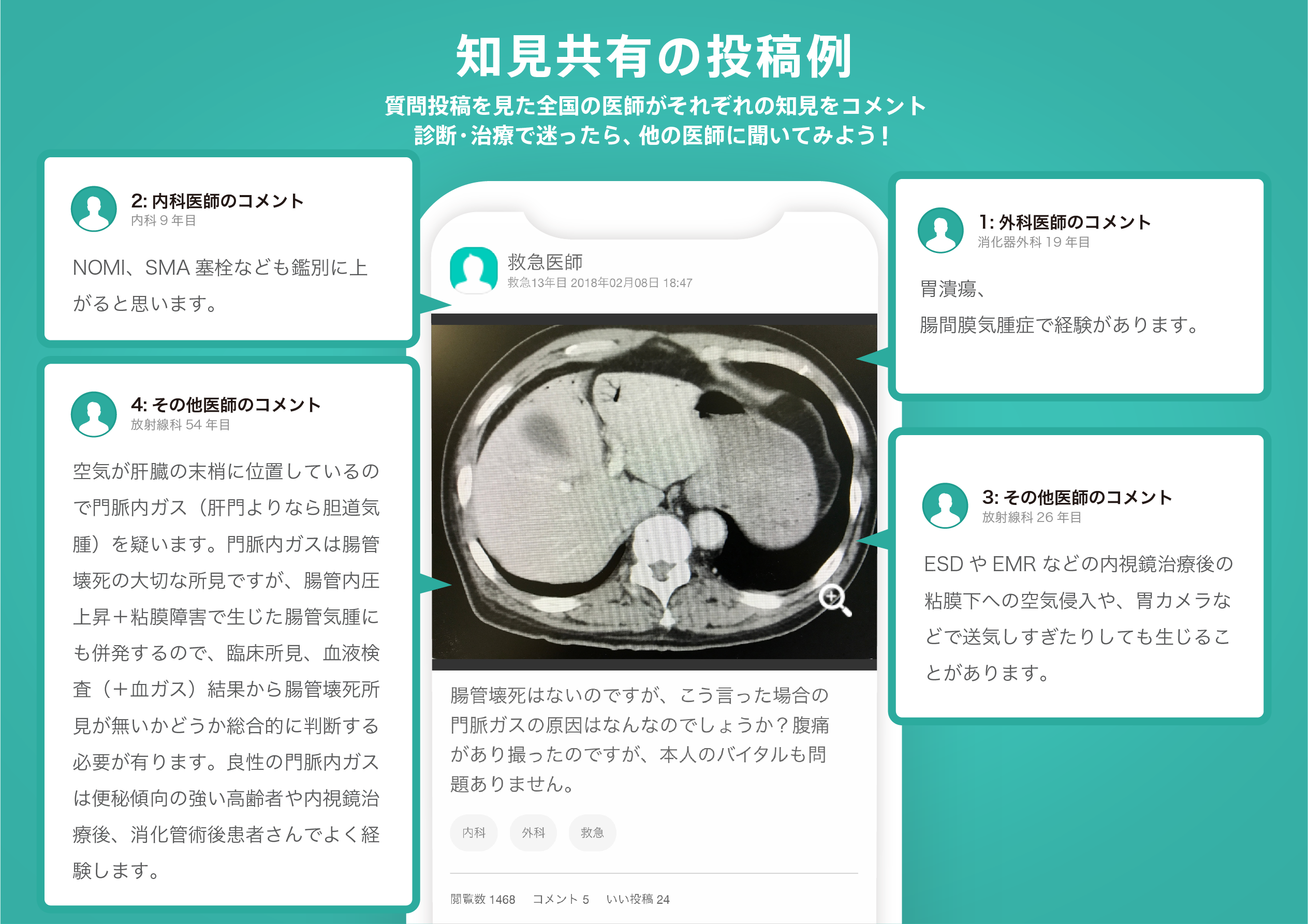
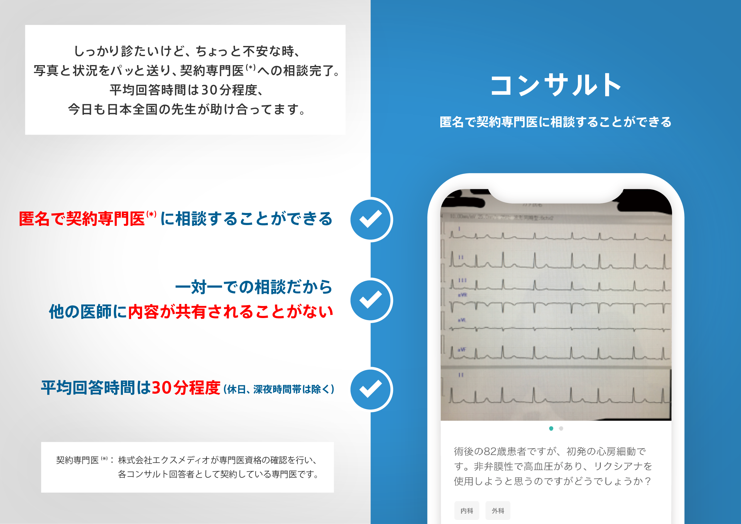
医師のための臨床サポートサービス
ヒポクラ x マイナビのご紹介

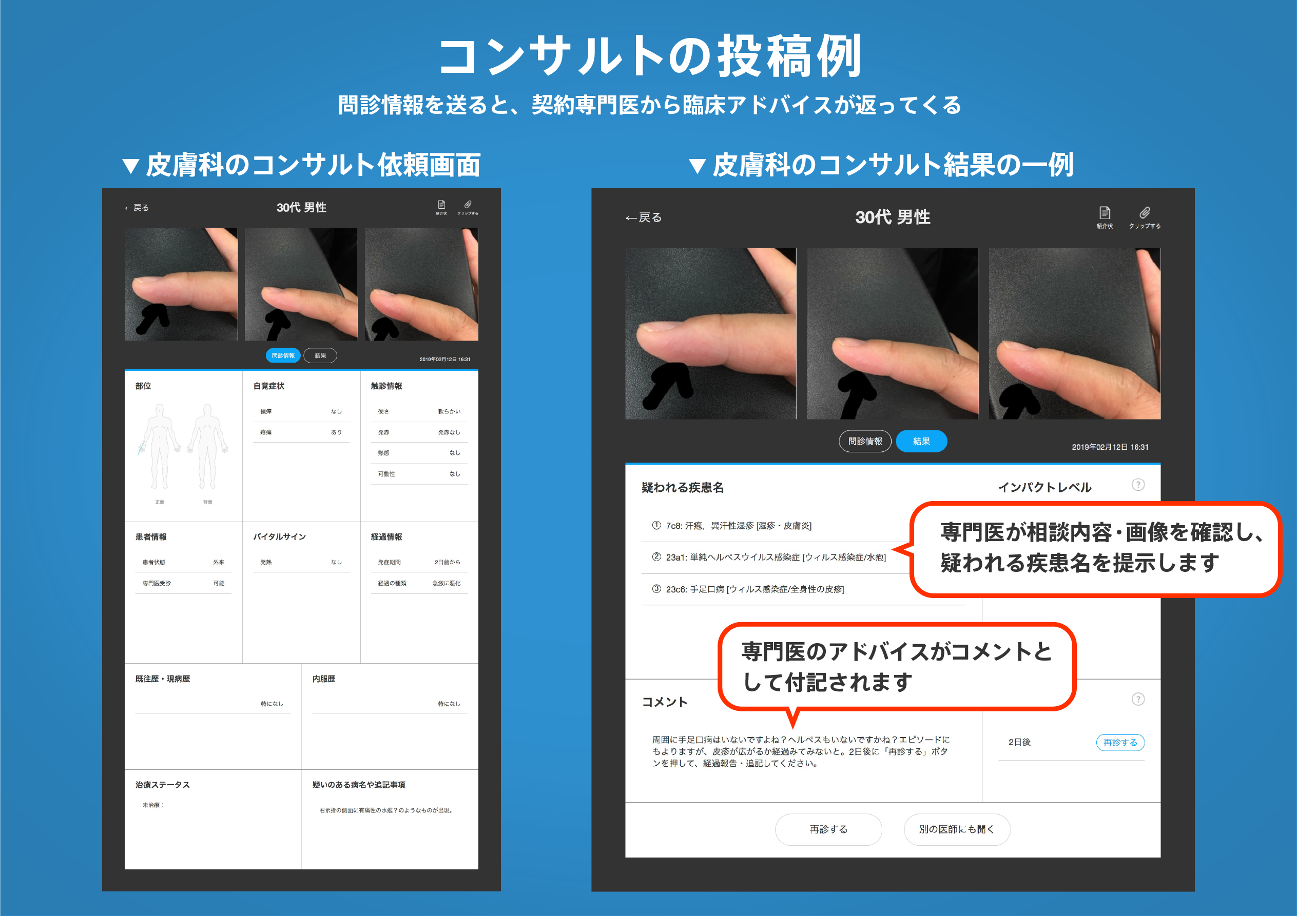
無料会員登録していただくと、さらに便利で効率的な検索が可能になります。