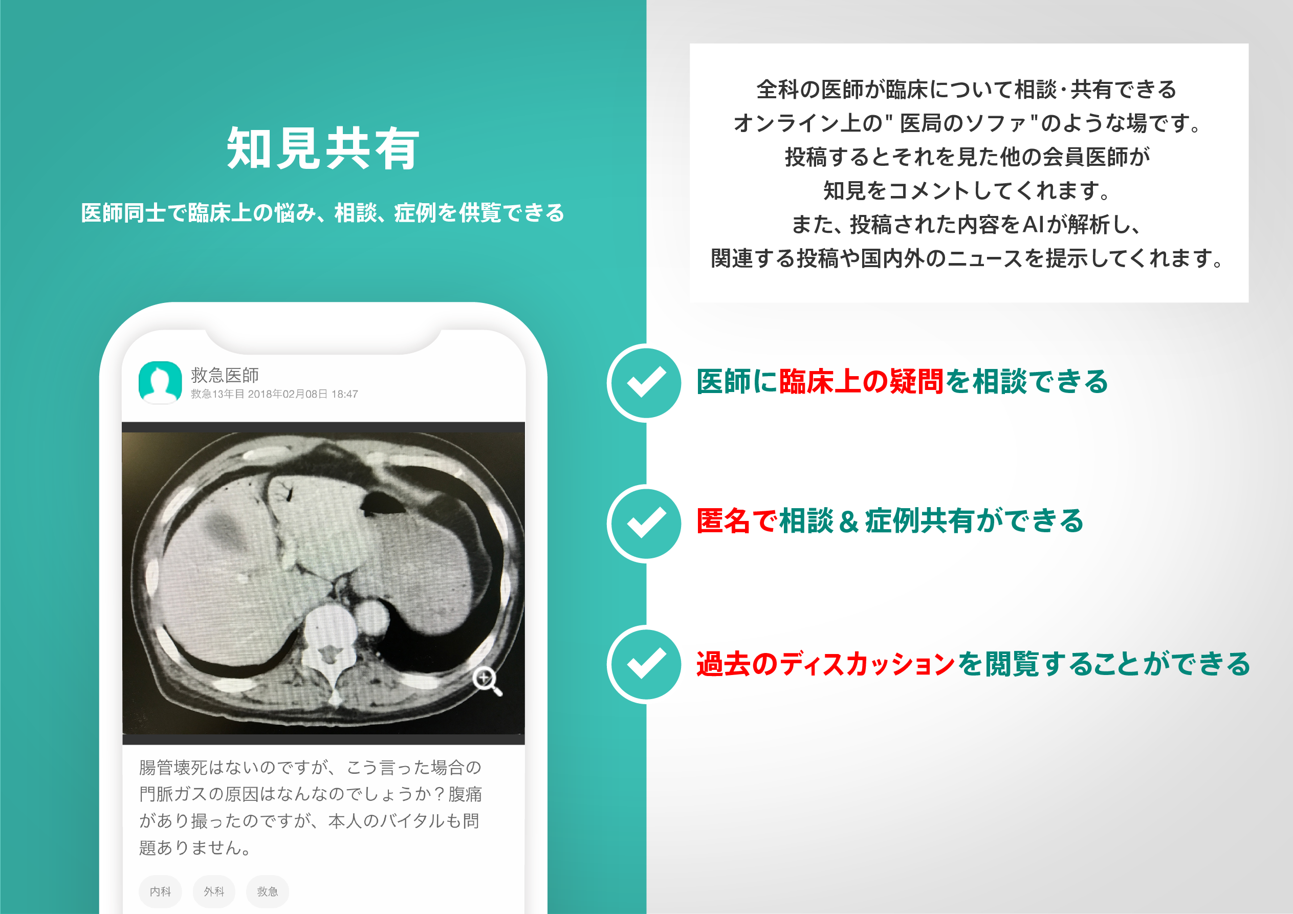
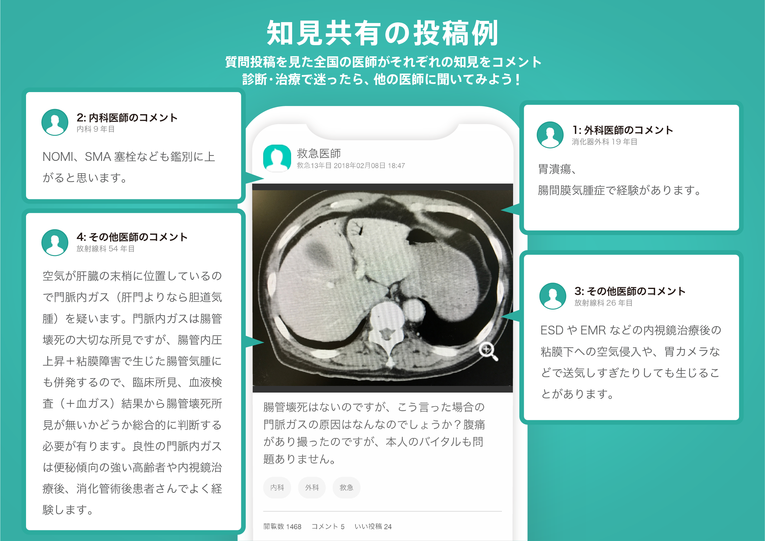
著名医師による解説が無料で読めます
すると翻訳の精度が向上します
大部分、多層、薄膜、高アスペクト比、層のバイアスと硬質基質間で結合できるオープンチャネルを備えた3Dマイクロ流体構造を製造するための新しい方法論を報告します。PDMS表面の下に埋め込まれた薄いプラスチックシートを備えたハイブリッドスタンプを使用することで実現されます。このハイブリッドスタンプは、PDMS成形中に重要なエッジ突起の問題を解決し、必要なスタンプの弾力性を維持し、層層領域でPDMS残基を除去することを保証します。エッジ突起を除去することは、高アスペクト比PDMS構造を備えた高アスペクト比PDMS構造を実現して、硬質基板への多層積み重ねと結合を促進できるため、3D構造の製造に向けた大きな進歩です。また、私たちの方法では、3D変形可能なチャネルの製造が可能になり、電気動物、光液、慣性マイクロ流体、およびチャネル断面の形状がデバイス物理学に重要な役割を果たす他のフィールドにおける重大なアプリケーションにつながる可能性があります。例として、2つの特徴のない伊藤ガラス基板の間に2つの20μm、高さ80μmのPDMS膜を挟むことにより、マイクロ流体チャネルを製造しました。2つのITO基質に電気バイアスを適用し、薄い膜の側壁を変形させる圧力をかけることにより、チャネルの中心で強力な電界増強を生成して、哺乳類細胞や細菌を含む生物学的物体の3Dシースレス誘電性焦点を流れの速度を上げることを可能にすることができます14 cm s(-1)。
大部分、多層、薄膜、高アスペクト比、層のバイアスと硬質基質間で結合できるオープンチャネルを備えた3Dマイクロ流体構造を製造するための新しい方法論を報告します。PDMS表面の下に埋め込まれた薄いプラスチックシートを備えたハイブリッドスタンプを使用することで実現されます。このハイブリッドスタンプは、PDMS成形中に重要なエッジ突起の問題を解決し、必要なスタンプの弾力性を維持し、層層領域でPDMS残基を除去することを保証します。エッジ突起を除去することは、高アスペクト比PDMS構造を備えた高アスペクト比PDMS構造を実現して、硬質基板への多層積み重ねと結合を促進できるため、3D構造の製造に向けた大きな進歩です。また、私たちの方法では、3D変形可能なチャネルの製造が可能になり、電気動物、光液、慣性マイクロ流体、およびチャネル断面の形状がデバイス物理学に重要な役割を果たす他のフィールドにおける重大なアプリケーションにつながる可能性があります。例として、2つの特徴のない伊藤ガラス基板の間に2つの20μm、高さ80μmのPDMS膜を挟むことにより、マイクロ流体チャネルを製造しました。2つのITO基質に電気バイアスを適用し、薄い膜の側壁を変形させる圧力をかけることにより、チャネルの中心で強力な電界増強を生成して、哺乳類細胞や細菌を含む生物学的物体の3Dシースレス誘電性焦点を流れの速度を上げることを可能にすることができます14 cm s(-1)。
We report a novel methodology for fabricating large-area, multilayer, thin-film, high aspect ratio, 3D microfluidic structures with through-layer vias and open channels that can be bonded between hard substrates. It is realized by utilizing a hybrid stamp with a thin plastic sheet embedded underneath a PDMS surface. This hybrid stamp solves an important edge protrusion issue during PDMS molding while maintaining necessary stamp elasticity to ensure the removal of PDMS residues at through-layer regions. Removing edge protrusion is a significant progress toward fabricating 3D structures since high aspect ratio PDMS structures with flat interfaces can be realized to facilitate multilayer stacking and bonding to hard substrates. Our method also allows for the fabrication of 3D deformable channels, which can lead to profound applications in electrokinetics, optofluidics, inertial microfluidics, and other fields where the shape of the channel cross section plays a key role in device physics. To demonstrate, as an example, we have fabricated a microfluidic channel by sandwiching two 20 μm wide, 80 μm tall PDMS membranes between two featureless ITO glass substrates. By applying electrical bias to the two ITO substrates and pressure to deform the thin membrane sidewalls, strong electric field enhancement can be generated in the center of a channel to enable 3D sheathless dielectrophoretic focusing of biological objects including mammalian cells and bacteria at a flow speed up to 14 cm s(-1).
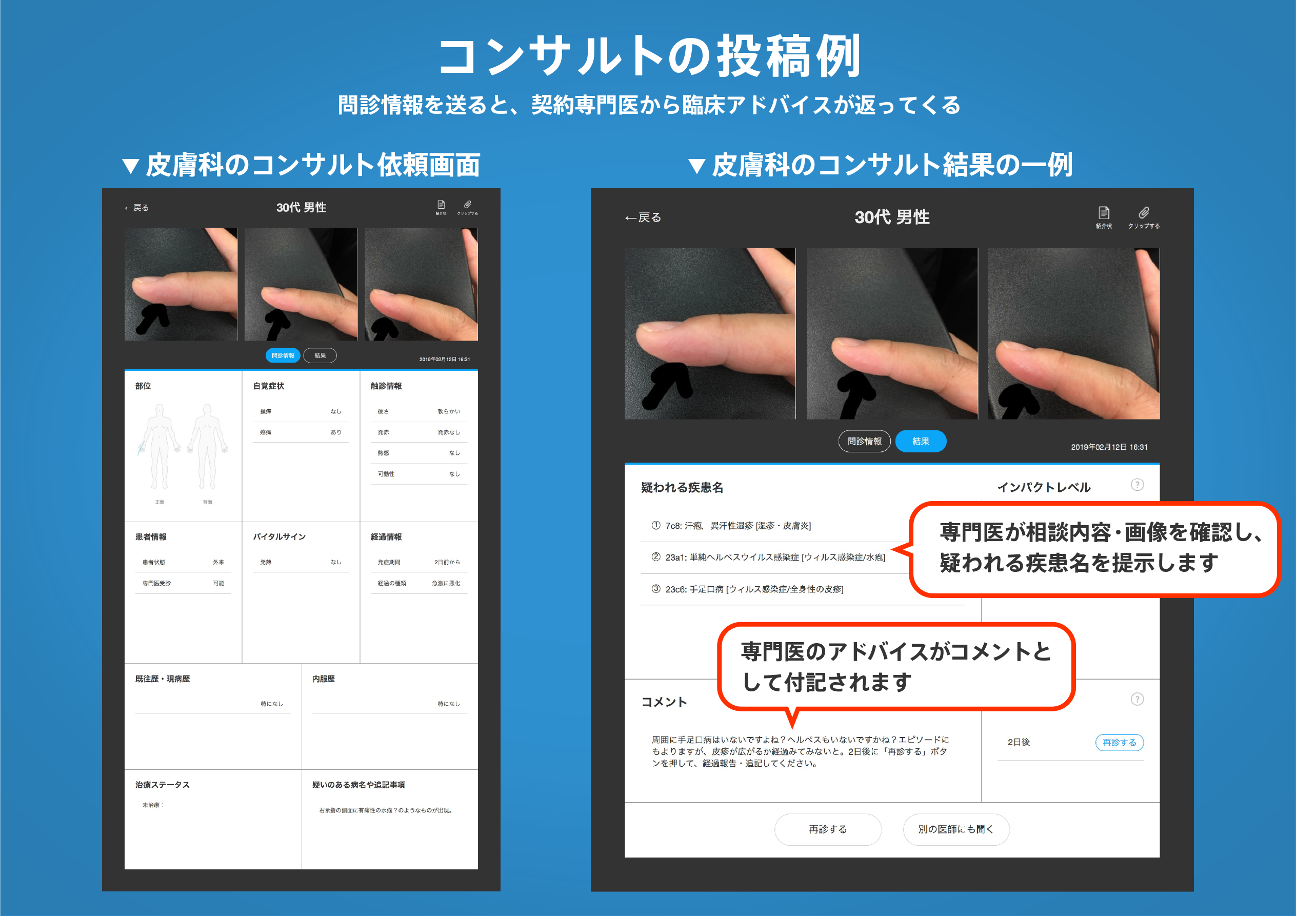
医師のための臨床サポートサービス
ヒポクラ x マイナビのご紹介


無料会員登録していただくと、さらに便利で効率的な検索が可能になります。