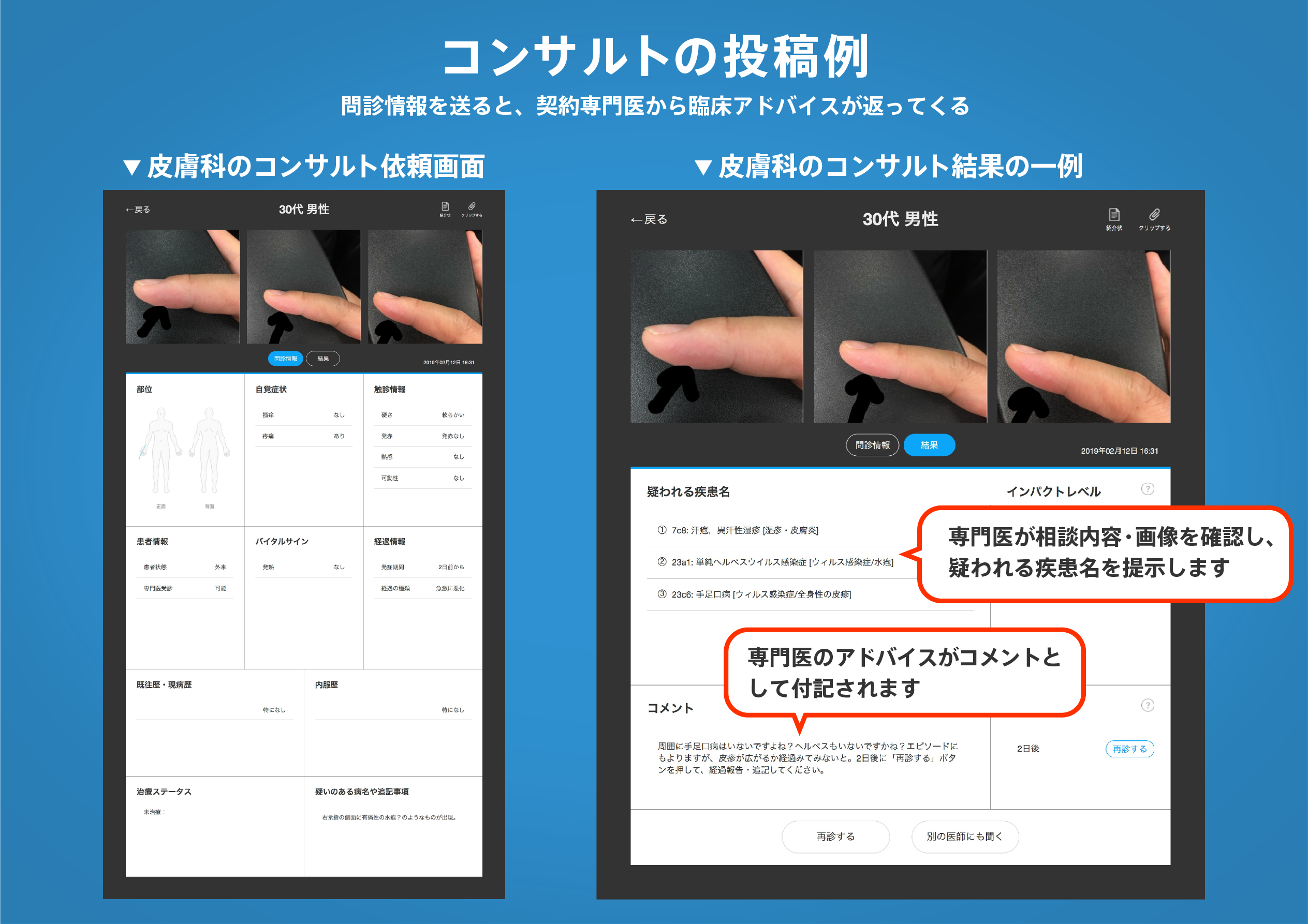
著名医師による解説が無料で読めます
すると翻訳の精度が向上します
二次元(2D)ヘテロ構造は、機能性が多様であるため、将来の原子的に薄いエレクトロニクスとオプトエレクトロニクスの約束を保持します。よく一致した格子と新規の物理的特性を持つさまざまな2D材料で構成されるヘテロ構造は、ファンデルワールス(VDW)エピタキシーを介して成功裏に製造されていますが、大きな格子の不適合を備えた層状半導体からヘテロ構造を構築しています。2段階の化学蒸気堆積(CVD)を使用した大きな格子ミスフィットを備えた2Dガス/Mose2ヘテロ構造の成長を報告します。垂直に積み重ねられたヘテロ構造と横方向の両方のヘテロ構造が実証されています。垂直に積み重ねられたガス/Mose2ヘテロ構造は、2つの層の間によく整列した格子配向を備えたVDWエピタキシーを示し、周期的な超格子を形成します。ただし、外側のヘテロ構造は、GaseとMose2の結晶ドメインの間の界面で外側のエピタキシャルアライメントを示しません。外側gase/mose2ヘテロ構造のガスとMose2単層ドメインの間に同じ格子配向が観察される境界領域での直接的な横方向の接続の代わりに、gase単層がCVD中にMose2を過剰成長させ、垂直にスタックされたvdwヘテロ構造のストライプを形成することがわかります。クリスタルインターフェイス。このような垂直に積み重ねられたVDWガス/MOSE2ヘテロ構造は、層間の光発生電荷キャリアの効果的な輸送と分離を伴うP-N接合を形成することが示されており、ゲート変動光電圧応答をもたらします。これらのGase/Mose2 VDWヘテロ構造には、ゲート変換可能なフィールド効果トランジスタ、フォトセクター、および太陽電池としてのアプリケーションが必要です。
二次元(2D)ヘテロ構造は、機能性が多様であるため、将来の原子的に薄いエレクトロニクスとオプトエレクトロニクスの約束を保持します。よく一致した格子と新規の物理的特性を持つさまざまな2D材料で構成されるヘテロ構造は、ファンデルワールス(VDW)エピタキシーを介して成功裏に製造されていますが、大きな格子の不適合を備えた層状半導体からヘテロ構造を構築しています。2段階の化学蒸気堆積(CVD)を使用した大きな格子ミスフィットを備えた2Dガス/Mose2ヘテロ構造の成長を報告します。垂直に積み重ねられたヘテロ構造と横方向の両方のヘテロ構造が実証されています。垂直に積み重ねられたガス/Mose2ヘテロ構造は、2つの層の間によく整列した格子配向を備えたVDWエピタキシーを示し、周期的な超格子を形成します。ただし、外側のヘテロ構造は、GaseとMose2の結晶ドメインの間の界面で外側のエピタキシャルアライメントを示しません。外側gase/mose2ヘテロ構造のガスとMose2単層ドメインの間に同じ格子配向が観察される境界領域での直接的な横方向の接続の代わりに、gase単層がCVD中にMose2を過剰成長させ、垂直にスタックされたvdwヘテロ構造のストライプを形成することがわかります。クリスタルインターフェイス。このような垂直に積み重ねられたVDWガス/MOSE2ヘテロ構造は、層間の光発生電荷キャリアの効果的な輸送と分離を伴うP-N接合を形成することが示されており、ゲート変動光電圧応答をもたらします。これらのGase/Mose2 VDWヘテロ構造には、ゲート変換可能なフィールド効果トランジスタ、フォトセクター、および太陽電池としてのアプリケーションが必要です。
Two-dimensional (2D) heterostructures hold the promise for future atomically thin electronics and optoelectronics because of their diverse functionalities. Although heterostructures consisting of different 2D materials with well-matched lattices and novel physical properties have been successfully fabricated via van der Waals (vdW) epitaxy, constructing heterostructures from layered semiconductors with large lattice misfits remains challenging. We report the growth of 2D GaSe/MoSe2 heterostructures with a large lattice misfit using two-step chemical vapor deposition (CVD). Both vertically stacked and lateral heterostructures are demonstrated. The vertically stacked GaSe/MoSe2 heterostructures exhibit vdW epitaxy with well-aligned lattice orientation between the two layers, forming a periodic superlattice. However, the lateral heterostructures exhibit no lateral epitaxial alignment at the interface between GaSe and MoSe2 crystalline domains. Instead of a direct lateral connection at the boundary region where the same lattice orientation is observed between GaSe and MoSe2 monolayer domains in lateral GaSe/MoSe2 heterostructures, GaSe monolayers are found to overgrow MoSe2 during CVD, forming a stripe of vertically stacked vdW heterostructures at the crystal interface. Such vertically stacked vdW GaSe/MoSe2 heterostructures are shown to form p-n junctions with effective transport and separation of photogenerated charge carriers between layers, resulting in a gate-tunable photovoltaic response. These GaSe/MoSe2 vdW heterostructures should have applications as gate-tunable field-effect transistors, photodetectors, and solar cells.
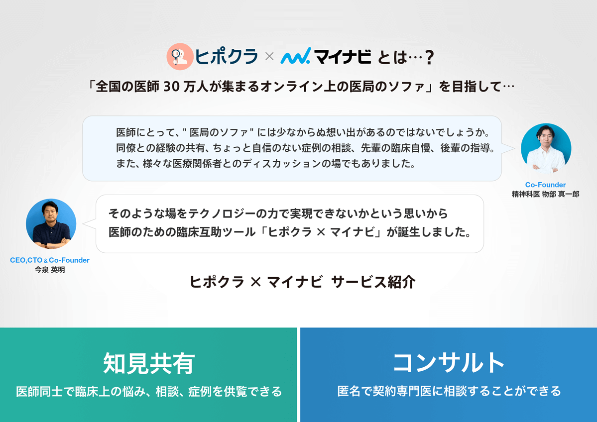
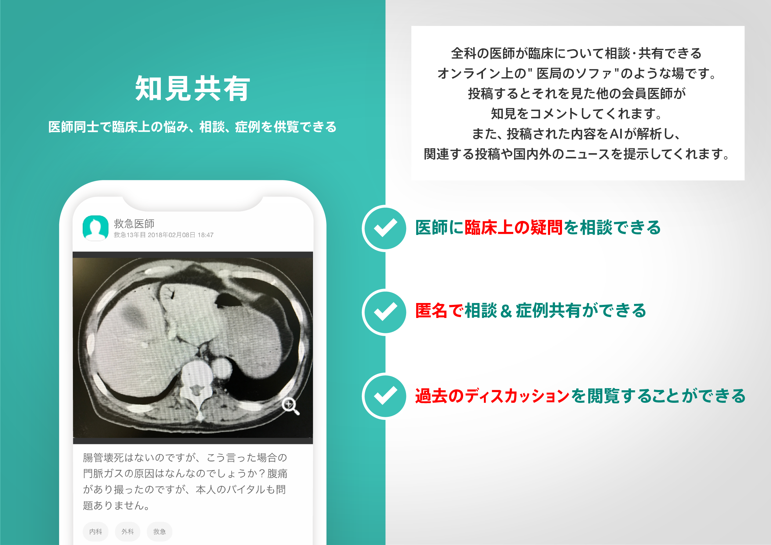
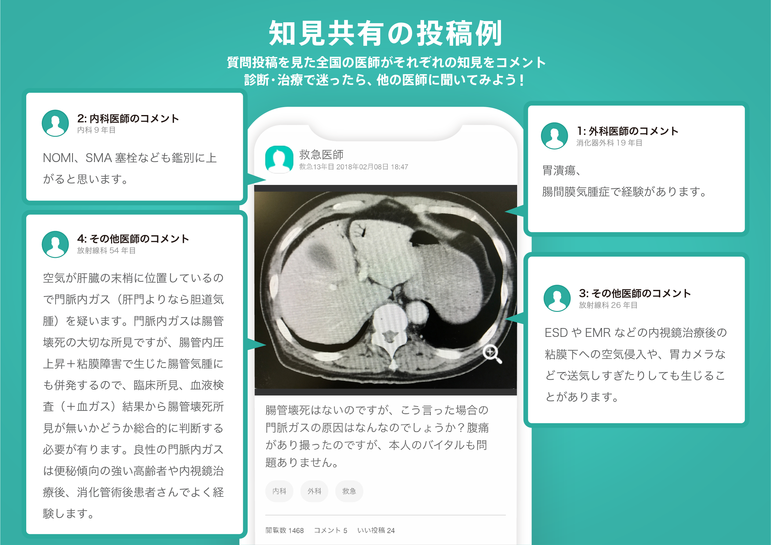
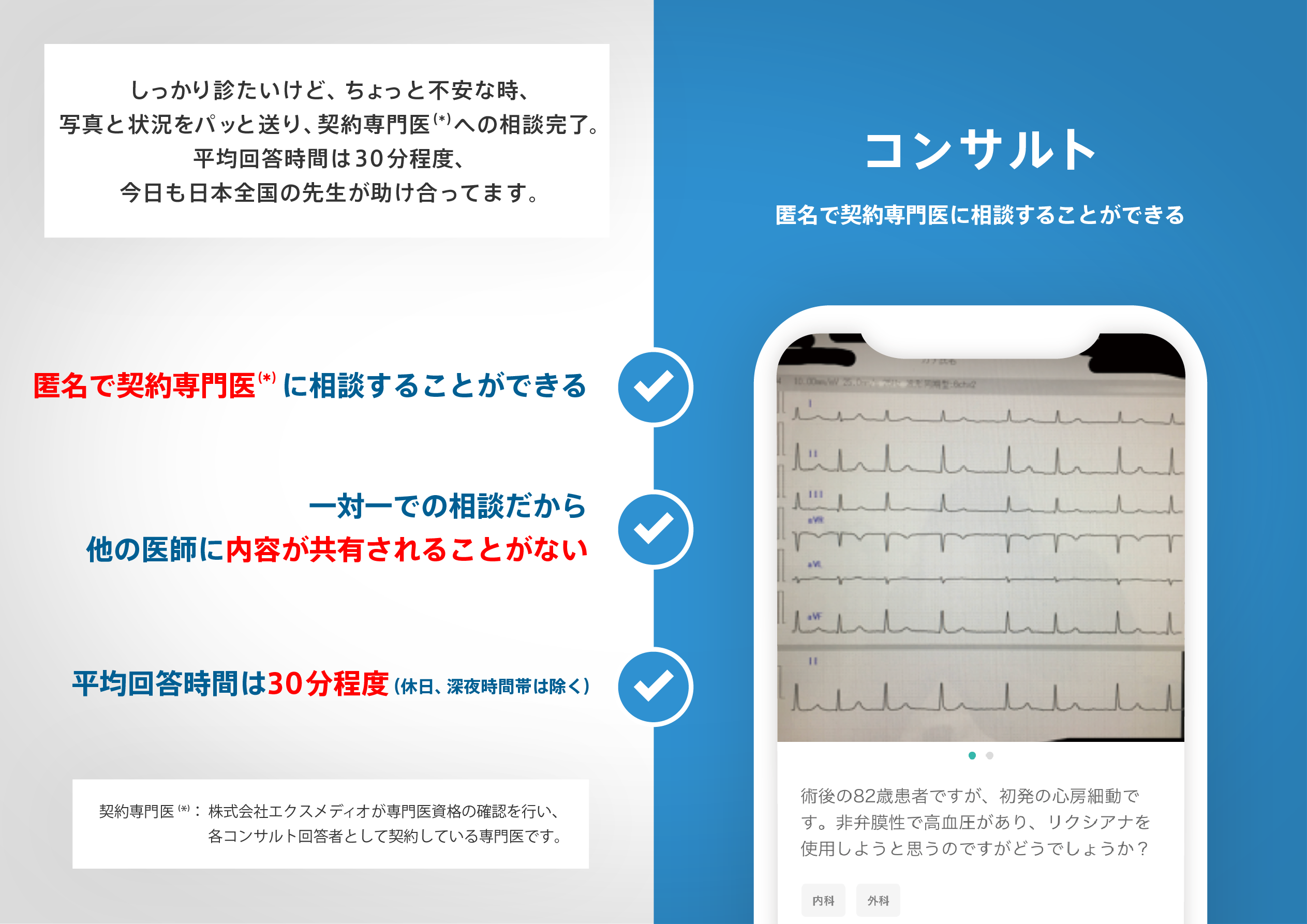
医師のための臨床サポートサービス
ヒポクラ x マイナビのご紹介

無料会員登録していただくと、さらに便利で効率的な検索が可能になります。