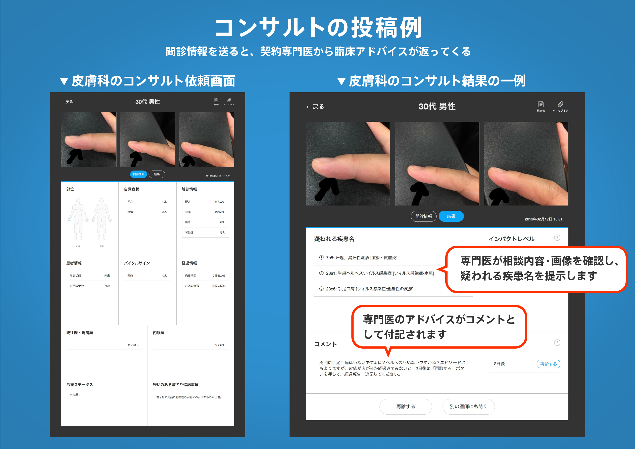
著名医師による解説が無料で読めます
すると翻訳の精度が向上します
この記事では、100°Cの単結晶シリコン上の酸化インジウムスズ(ITO)材料の制御可能なマグネトロンスパッタリングを使用して、ITO/A-SIOX/N-SIの光電子ヘテロ接合フレームは、単に実現する目的で単に製造されます。不動態化の接触と穴のトンネル。ITOとN-SIの間の超薄膜境界ゾーン内の酸化シリコン(SIOX/IN)とともに、インジウム(IN)要素の勾配プロファイルが発生し、イオンミリング技術を備えたX線光電子分光法によって特徴付けられることがわかります。界面層の原子形態と物理相は、高解像度透過電子顕微鏡で観察されています。X線回折、ホール効果測定、およびTAUCプロットによる光学透過率は、それぞれITO薄膜の微細構造および特性分析に適用されています。多結晶相とアモルファス相は、それぞれITOフィルムとSIOX(IN)ハイブリッド層で検証されています。量子輸送の場合、A-Siox(In)層を介した光発生穴の直接および欠陥支援トンネルの両方が確認されています。さらに、インジウム組成に相関するギャップ状態があり、第一原理計算の密度官能理論によって予測される三元ハイブリッドA-Siox(in)層のEV + 4.60 eVに位置します。状態 "光生成穴の直接トンネルのため。合理的な組み込みのポテンシャル(VBI = 0.66 V)および最適に制御された三元ハイブリッドA-Siox(IN)層(約1.4 nm)は、デバイスが0.540 V、A A A 0.540 Vの優れたPVパフォーマンスを示し、AM 1.5照明下では、30.5 mA/cm2の短絡電流密度、74.2%の高い充填係数、12.2%の変換効率。ITO(5.06 eV)とN-Si(4.31 eV)の作業関数の違いは、紫外線光排出分光法によって決定され、PVデバイスの組み込みフィールドの本質に起因します。さらに、N-Si基質の表面における強い反転層は、A-Siox(In)界面層とも同様に相関しています。
この記事では、100°Cの単結晶シリコン上の酸化インジウムスズ(ITO)材料の制御可能なマグネトロンスパッタリングを使用して、ITO/A-SIOX/N-SIの光電子ヘテロ接合フレームは、単に実現する目的で単に製造されます。不動態化の接触と穴のトンネル。ITOとN-SIの間の超薄膜境界ゾーン内の酸化シリコン(SIOX/IN)とともに、インジウム(IN)要素の勾配プロファイルが発生し、イオンミリング技術を備えたX線光電子分光法によって特徴付けられることがわかります。界面層の原子形態と物理相は、高解像度透過電子顕微鏡で観察されています。X線回折、ホール効果測定、およびTAUCプロットによる光学透過率は、それぞれITO薄膜の微細構造および特性分析に適用されています。多結晶相とアモルファス相は、それぞれITOフィルムとSIOX(IN)ハイブリッド層で検証されています。量子輸送の場合、A-Siox(In)層を介した光発生穴の直接および欠陥支援トンネルの両方が確認されています。さらに、インジウム組成に相関するギャップ状態があり、第一原理計算の密度官能理論によって予測される三元ハイブリッドA-Siox(in)層のEV + 4.60 eVに位置します。状態 "光生成穴の直接トンネルのため。合理的な組み込みのポテンシャル(VBI = 0.66 V)および最適に制御された三元ハイブリッドA-Siox(IN)層(約1.4 nm)は、デバイスが0.540 V、A A A 0.540 Vの優れたPVパフォーマンスを示し、AM 1.5照明下では、30.5 mA/cm2の短絡電流密度、74.2%の高い充填係数、12.2%の変換効率。ITO(5.06 eV)とN-Si(4.31 eV)の作業関数の違いは、紫外線光排出分光法によって決定され、PVデバイスの組み込みフィールドの本質に起因します。さらに、N-Si基質の表面における強い反転層は、A-Siox(In)界面層とも同様に相関しています。
In this article, using controllable magnetron sputtering of indium tin oxide (ITO) materials on single crystal silicon at 100 °C, the optoelectronic heterojunction frame of ITO/a-SiOx(In)/n-Si is simply fabricated for the purpose of realizing passivation contact and hole tunneling. It is found that the gradation profile of indium (In) element together with silicon oxide (SiOx/In) within the ultrathin boundary zone between ITO and n-Si occurs and is characterized by X-ray photoelectron spectroscopy with the ion milling technique. The atomistic morphology and physical phase of the interfacial layer has been observed with a high-resolution transmission electron microscope. X-ray diffraction, Hall effect measurement, and optical transmittance with Tauc plot have been applied to the microstructure and property analyses of ITO thin films, respectively. The polycrystalline and amorphous phases have been verified for ITO films and SiOx(In) hybrid layer, respectively. For the quantum transport, both direct and defect-assisted tunneling of photogenerated holes through the a-SiOx(In) layer is confirmed. Besides, there is a gap state correlative to the indium composition and located at Ev + 4.60 eV in the ternary hybrid a-SiOx(In) layer that is predicted by density functional theory of first-principles calculation, which acts as an "extended delocalized state" for direct tunneling of the photogenerated holes. The reasonable built-in potential (Vbi = 0.66 V) and optimally controlled ternary hybrid a-SiOx(In) layer (about 1.4 nm) result in that the device exhibits excellent PV performance, with an open-circuit voltage of 0.540 V, a short-circuit current density of 30.5 mA/cm2, a high fill factor of 74.2%, and a conversion efficiency of 12.2%, under the AM 1.5 illumination. The work function difference between ITO (5.06 eV) and n-Si (4.31 eV) is determined by ultraviolet photoemission spectroscopy and ascribed to the essence of the built-in-field of the PV device. In addition, the strong inversion layer in the surface of the n-Si substrate is tentatively correlated to the a-SiOx(In) interface layer as well.
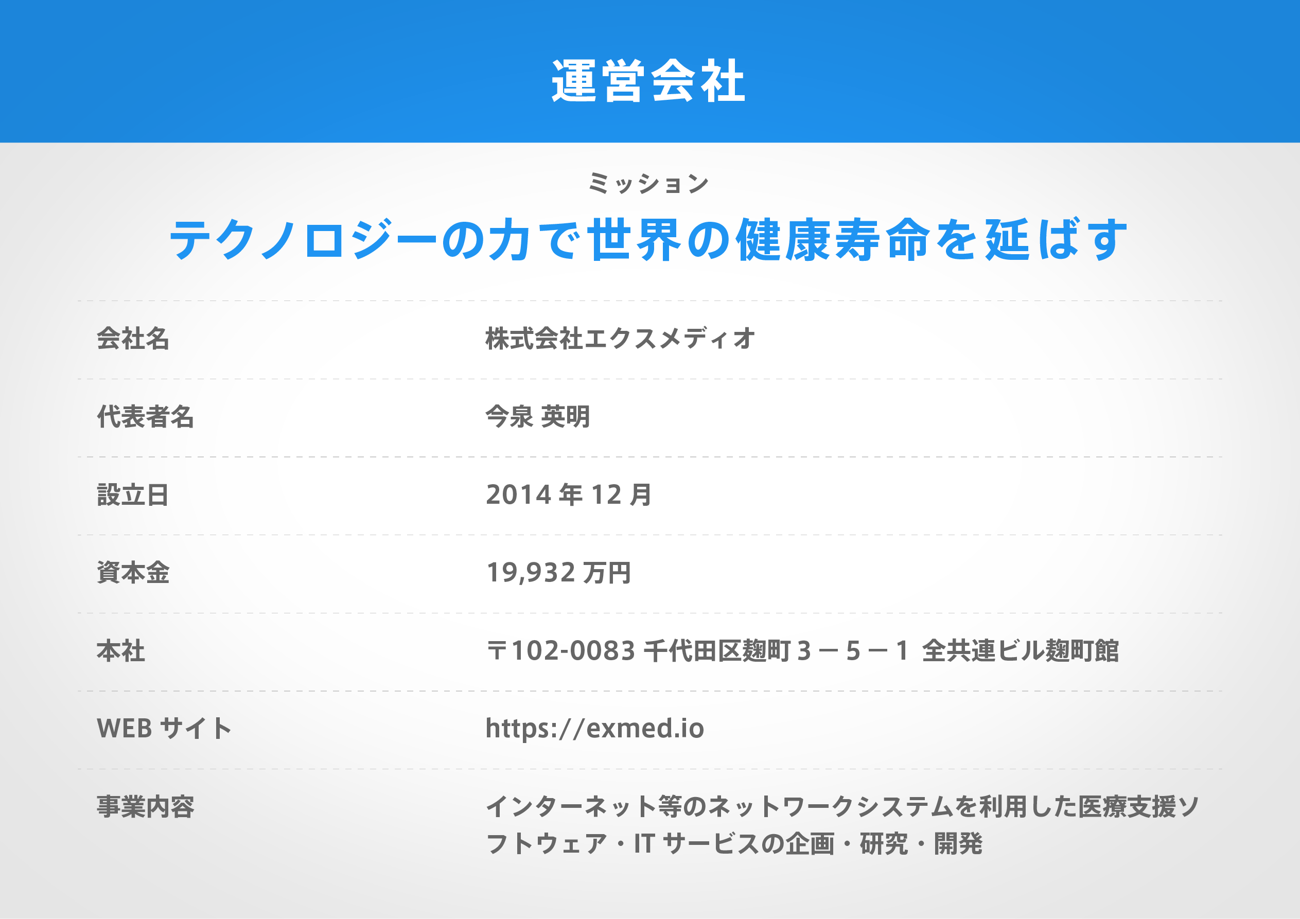
医師のための臨床サポートサービス
ヒポクラ x マイナビのご紹介


無料会員登録していただくと、さらに便利で効率的な検索が可能になります。