著名医師による解説が無料で読めます
すると翻訳の精度が向上します
変成および光電子特性は、変成および従来の偽モルフィックINAS/GAAS量子ドット(QD)構造の光学的特性を研究しました。2つの異なる電気接触構成を使用して、(i)QDと埋め込み層を介してのみ、(ii)GAAS基質(Wafer)を含むすべての構造を介して(ii)介してのみを使用しました。QDの状態、湿潤層、GAASまたはINGAASバッファー、および欠陥関連センターの間の異なる光学遷移は、光電圧(PV)、光導管(PC)、フォトルミネッセンス(PL)、および吸収分光法によって研究されました。INGAASバッファーの使用は、QD PLバンドの最大値を、収量を減らすことなく1.3μm(通信範囲)にスペクトル的にシフトすることが示されました。変成QDの光感受性はGAASバッファーの光感度よりも高いことがわかりましたが、変成型および偽型バッファー層の両方の光検査結果は類似していました。PVとPCのメカニズムは、両方の構造について議論されました。研究された構造の特性の非類似性は、異なる設計の観点から説明されています。両方の構造の光電気特性に対する欠陥の重要な影響は、接触構成(II)のために0.68〜1.0 eVのスペクトル範囲で、つまり電動活性GAASウェーハの場合に観察されました。構造が上部および下部バッファーに接触した場合、構成(i)には光電スペクトルに対するそのような欠陥の影響は見つかりませんでした。擬似動態構造の光電流スペクトルで観察され、INAS/GAAS QDに近い欠陥に関連していると解釈される0.83 EV特徴のみが観察されました。
変成および光電子特性は、変成および従来の偽モルフィックINAS/GAAS量子ドット(QD)構造の光学的特性を研究しました。2つの異なる電気接触構成を使用して、(i)QDと埋め込み層を介してのみ、(ii)GAAS基質(Wafer)を含むすべての構造を介して(ii)介してのみを使用しました。QDの状態、湿潤層、GAASまたはINGAASバッファー、および欠陥関連センターの間の異なる光学遷移は、光電圧(PV)、光導管(PC)、フォトルミネッセンス(PL)、および吸収分光法によって研究されました。INGAASバッファーの使用は、QD PLバンドの最大値を、収量を減らすことなく1.3μm(通信範囲)にスペクトル的にシフトすることが示されました。変成QDの光感受性はGAASバッファーの光感度よりも高いことがわかりましたが、変成型および偽型バッファー層の両方の光検査結果は類似していました。PVとPCのメカニズムは、両方の構造について議論されました。研究された構造の特性の非類似性は、異なる設計の観点から説明されています。両方の構造の光電気特性に対する欠陥の重要な影響は、接触構成(II)のために0.68〜1.0 eVのスペクトル範囲で、つまり電動活性GAASウェーハの場合に観察されました。構造が上部および下部バッファーに接触した場合、構成(i)には光電スペクトルに対するそのような欠陥の影響は見つかりませんでした。擬似動態構造の光電流スペクトルで観察され、INAS/GAAS QDに近い欠陥に関連していると解釈される0.83 EV特徴のみが観察されました。
Optical and photoelectric properties of metamorphic InAs/InGaAs and conventional pseudomorphic InAs/GaAs quantum dot (QD) structures were studied. We used two different electrical contact configurations that allowed us to have the current flow (i) only through QDs and embedding layers and (ii) through all the structure, including the GaAs substrate (wafer). Different optical transitions between states of QDs, wetting layers, GaAs or InGaAs buffers, and defect-related centers were studied by means of photovoltage (PV), photoconductivity (PC), photoluminescence (PL), and absorption spectroscopies. It was shown that the use of the InGaAs buffer spectrally shifted the maximum of the QD PL band to 1.3 μm (telecommunication range) without a decrease in the yield. Photosensitivity for the metamorphic QDs was found to be higher than that in GaAs buffer while the photoresponses for both metamorphic and pseudomorphic buffer layers were similar. The mechanisms of PV and PC were discussed for both structures. The dissimilarities in properties of the studied structures are explained in terms of the different design. A critical influence of the defects on the photoelectrical properties of both structures was observed in the spectral range from 0.68 to 1.0 eV for contact configuration (ii), i.e., in the case of electrically active GaAs wafer. No effect of such defects on the photoelectric spectra was found for configuration (i), when the structures were contacted to the top and bottom buffers; only a 0.83 eV feature was observed in the photocurrent spectrum of pseudomorphic structure and interpreted to be related to defects close to InAs/GaAs QDs.
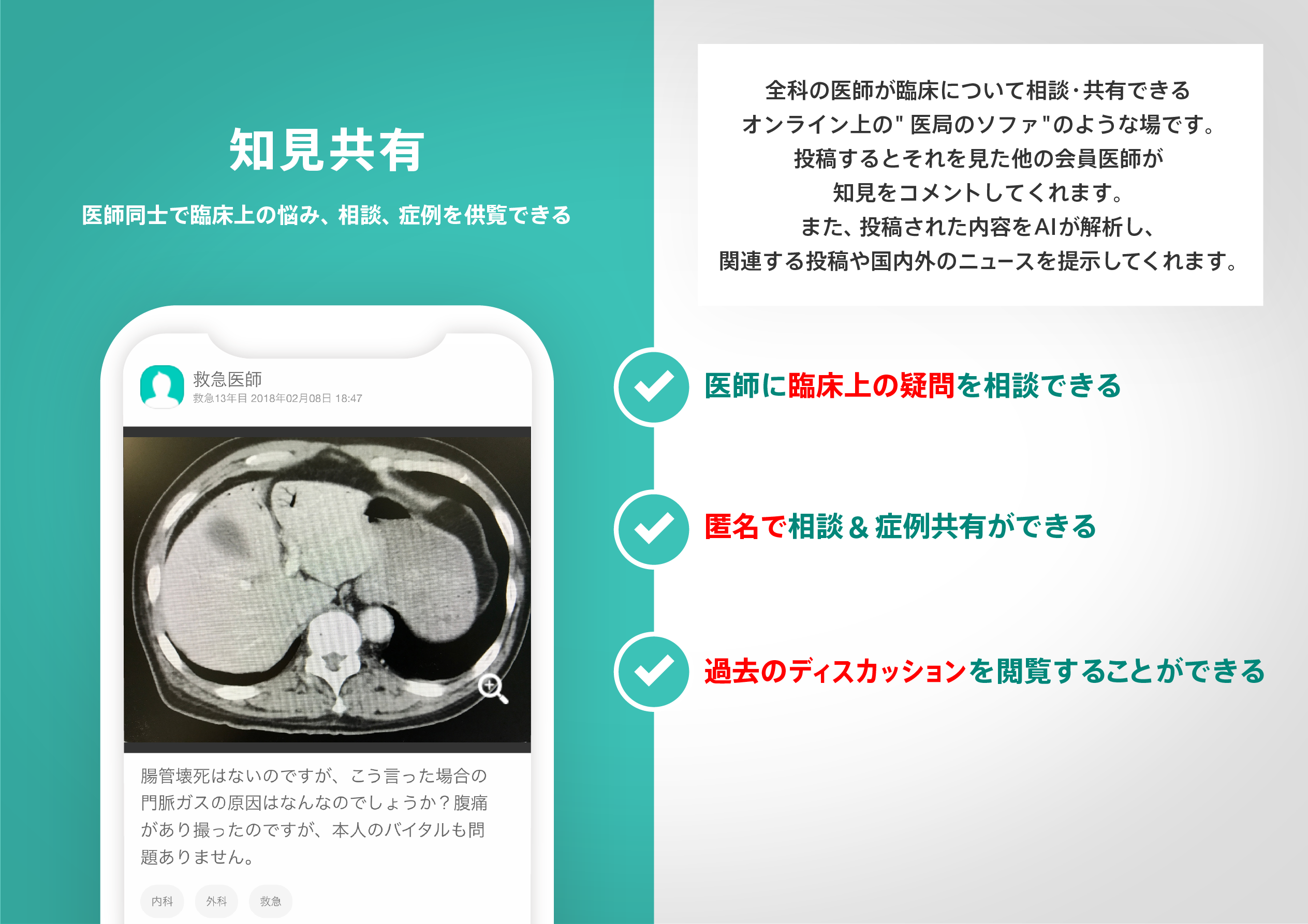
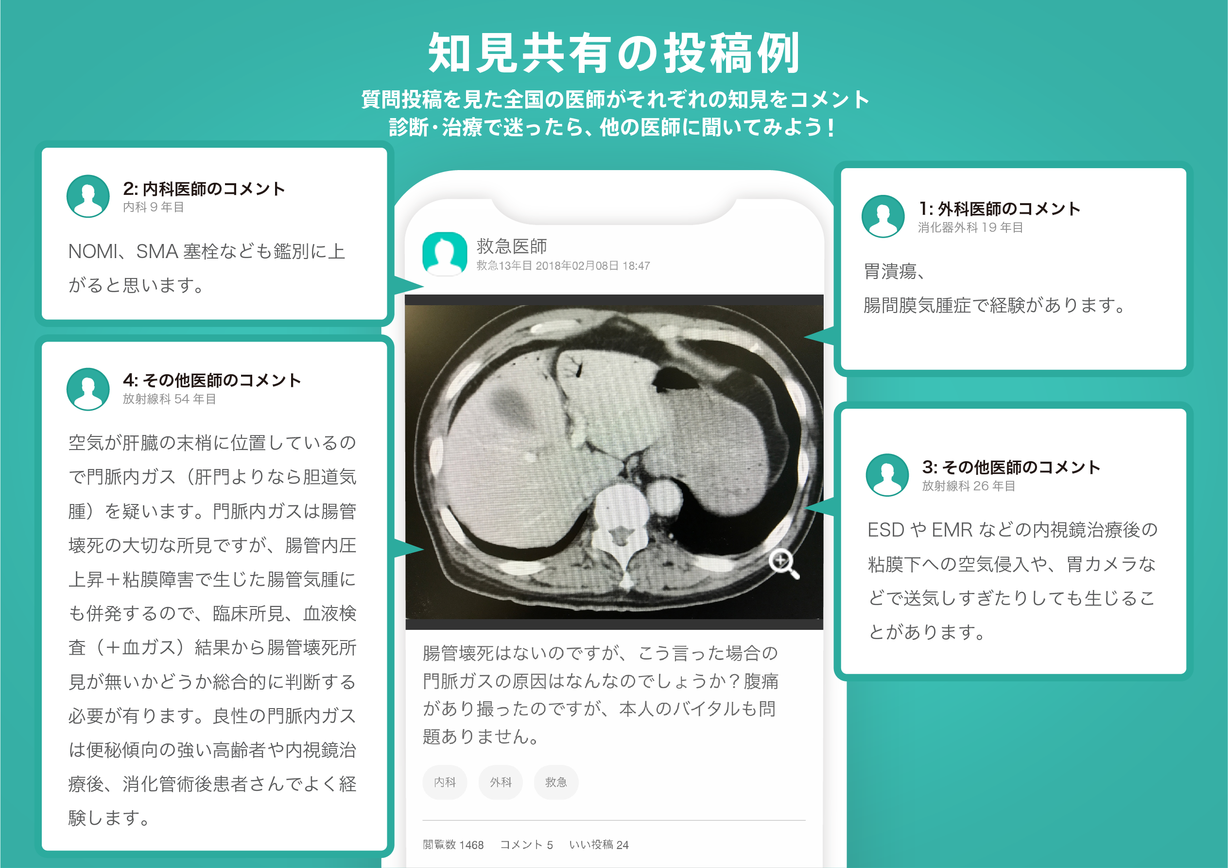
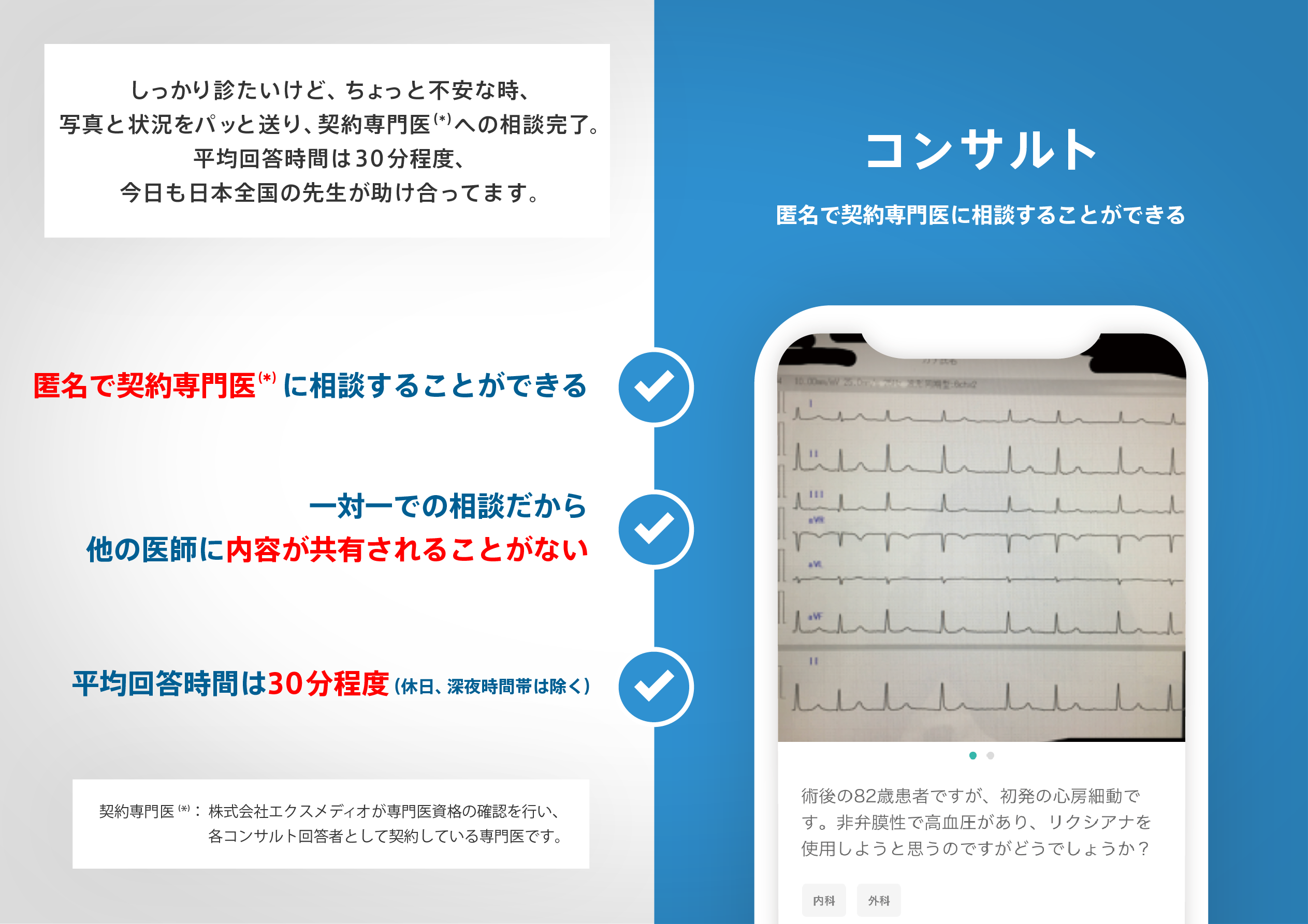
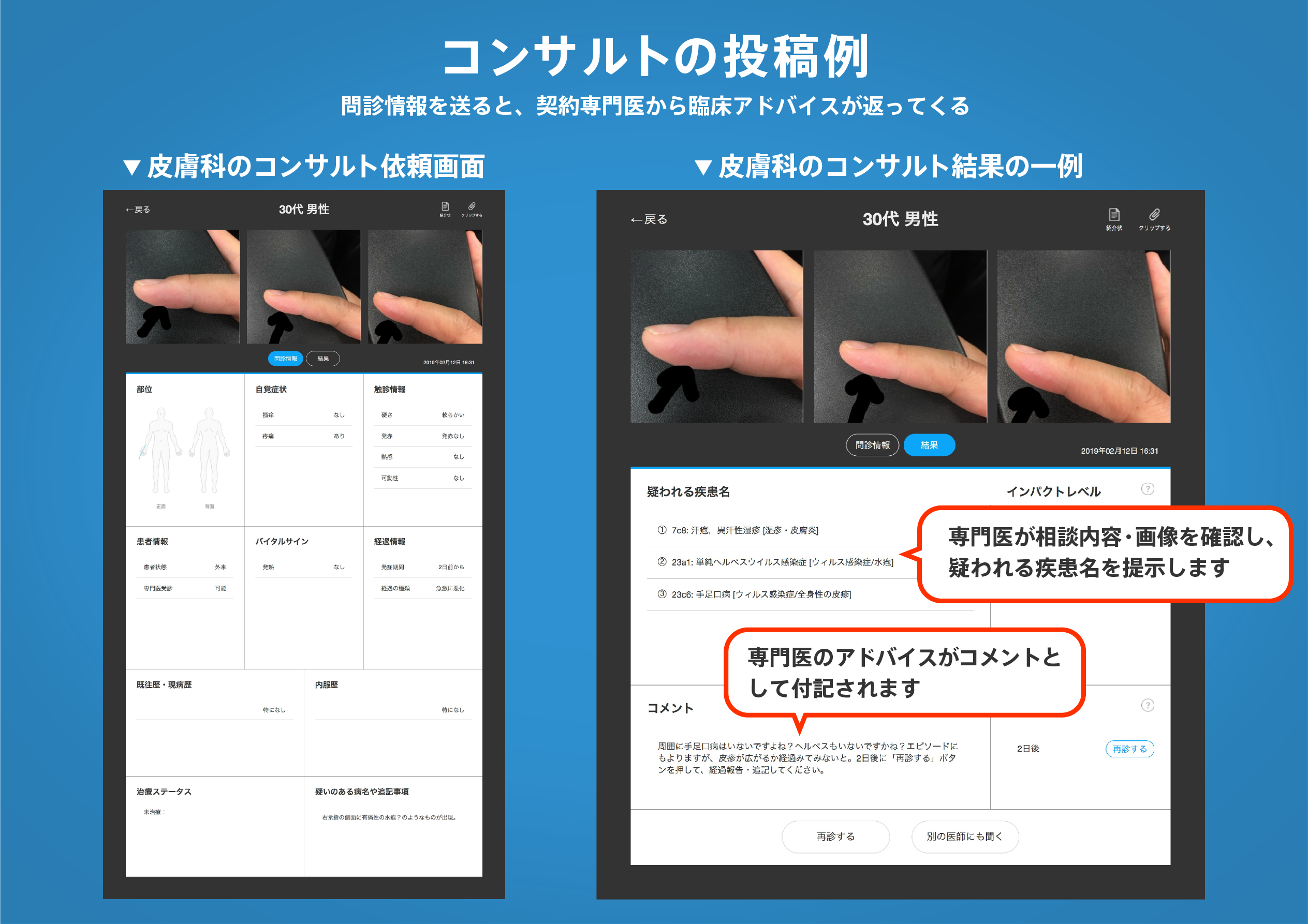
医師のための臨床サポートサービス
ヒポクラ x マイナビのご紹介


無料会員登録していただくと、さらに便利で効率的な検索が可能になります。