著名医師による解説が無料で読めます
すると翻訳の精度が向上します
有機ドナーacceptor(DA)複合体は、ここ数十年で幅広い注目を集めており、その結果、有機バイナリシステムの電子機器が急速に発展しています。さまざまな成分構造を備えた有機DA複合体の設計と合成は、主に金属性(または超伝導性)、放出、または強誘電性研究に焦点を合わせています。高性能の電子調査にさらなる努力が払われています。有機半導体の化学的汎用性により、DA複合体は、半導体アプリケーションに非常に多くの可能性を提供します。有機DA複合体は半導体ファミリーを拡張し、有機電界効果トランジスタ(OFET)および有機太陽光発電(OPV)での電荷分離と輸送を促進します。ofetsでは、有機錯体は並外れた電荷経路を横切る活性層として機能し、誘導電荷の効率的な輸送を保証します。よりますます多くの有機半導体が報告されていますが、優れたpまたはn型特性(1または10 cm2 V-1 S-1を超えるモビリティ)を示すことが報告されていますが、重要な科学的課題は、既存の半導体材料の利点を利用することに残っています。あまり複雑ではない合成またはデバイスの製造プロセスを維持しながら、より広くアプリケーション。DA複合材料は、新しい洞察を明らかにしました:それらの独自の分子包装と構造とプロパティの関係。ドナーとアクセプターの組み合わせは、単一分子材料と比較して実際的な利点を提供できます。第一に、密に詰まった構造を備えたDA複合体の結晶の成長は、自己組織化プロセスから不純物とトラップを減らします。第二に、元の構造成分に基づいた複合体は、優れた混合物積み重ねを形成する可能性があり、これにより、コセンブルプロセスの駆動力に応じて電荷輸送を促進できます。第三に、有機半導体の効果的な使用により、調整可能なバンド構造につながる可能性があり、トランジスタの動作モード(Pまたはn型)をコンポーネントを変更することで体系的に制御できます。最後に、ユニークなスタッキングを備えた共結晶に基づいた理論的計算は、構造とプロパティの関係の理解を広げ、DA複合体に基づいて高性能半導体を設計するのに役立ちます。このアカウントでは、有機DA複合体を、設計、成長方法、パッキングモード、充電輸送特性、構造とプロパティの関係など、新しいクラスの半導体材料として議論することに焦点を当てています。また、これらのバイナリ結晶に基づいてデバイスを製造および調査しました。この学際的な仕事は、自己組織化、結晶学、凝縮された物理学、および理論化学の分野からの技術を組み合わせています。研究者は、ドナーとアクセプター化合物を含む新しい複雑なシステムを設計しました。これは、実行可能な方法で高度に秩序化された共結晶に自己組織化されます。この結晶化方法を使用すると、偏極または単極輸送が簡単に実現できることを実証します。デバイスのパフォーマンスをさらに向上させるために、新しい種類のドナーとアクセプターの使用、ドナー(イオン化電位、IP)およびアクセプター(電子親和性、EA)コンポーネントのエネルギーアラインメントの変調、π-の拡張など、いくつかの設計戦略を提案します。共役バックボーン。さらに、分子の「ドーピング」(2:1共結晶化)を使用すると、有機半導体の電荷輸送の性質は、ホール輸送ポートが支配的に支配的に切り替えることができることがわかりました。有機ドナーとアクセプター種の錯化による共結晶の形成は、対応する個々の成分よりも優れたパフォーマンスを備えた有機電子機器の半導体を開発するための新しい戦略として役立つと予想しています。
有機ドナーacceptor(DA)複合体は、ここ数十年で幅広い注目を集めており、その結果、有機バイナリシステムの電子機器が急速に発展しています。さまざまな成分構造を備えた有機DA複合体の設計と合成は、主に金属性(または超伝導性)、放出、または強誘電性研究に焦点を合わせています。高性能の電子調査にさらなる努力が払われています。有機半導体の化学的汎用性により、DA複合体は、半導体アプリケーションに非常に多くの可能性を提供します。有機DA複合体は半導体ファミリーを拡張し、有機電界効果トランジスタ(OFET)および有機太陽光発電(OPV)での電荷分離と輸送を促進します。ofetsでは、有機錯体は並外れた電荷経路を横切る活性層として機能し、誘導電荷の効率的な輸送を保証します。よりますます多くの有機半導体が報告されていますが、優れたpまたはn型特性(1または10 cm2 V-1 S-1を超えるモビリティ)を示すことが報告されていますが、重要な科学的課題は、既存の半導体材料の利点を利用することに残っています。あまり複雑ではない合成またはデバイスの製造プロセスを維持しながら、より広くアプリケーション。DA複合材料は、新しい洞察を明らかにしました:それらの独自の分子包装と構造とプロパティの関係。ドナーとアクセプターの組み合わせは、単一分子材料と比較して実際的な利点を提供できます。第一に、密に詰まった構造を備えたDA複合体の結晶の成長は、自己組織化プロセスから不純物とトラップを減らします。第二に、元の構造成分に基づいた複合体は、優れた混合物積み重ねを形成する可能性があり、これにより、コセンブルプロセスの駆動力に応じて電荷輸送を促進できます。第三に、有機半導体の効果的な使用により、調整可能なバンド構造につながる可能性があり、トランジスタの動作モード(Pまたはn型)をコンポーネントを変更することで体系的に制御できます。最後に、ユニークなスタッキングを備えた共結晶に基づいた理論的計算は、構造とプロパティの関係の理解を広げ、DA複合体に基づいて高性能半導体を設計するのに役立ちます。このアカウントでは、有機DA複合体を、設計、成長方法、パッキングモード、充電輸送特性、構造とプロパティの関係など、新しいクラスの半導体材料として議論することに焦点を当てています。また、これらのバイナリ結晶に基づいてデバイスを製造および調査しました。この学際的な仕事は、自己組織化、結晶学、凝縮された物理学、および理論化学の分野からの技術を組み合わせています。研究者は、ドナーとアクセプター化合物を含む新しい複雑なシステムを設計しました。これは、実行可能な方法で高度に秩序化された共結晶に自己組織化されます。この結晶化方法を使用すると、偏極または単極輸送が簡単に実現できることを実証します。デバイスのパフォーマンスをさらに向上させるために、新しい種類のドナーとアクセプターの使用、ドナー(イオン化電位、IP)およびアクセプター(電子親和性、EA)コンポーネントのエネルギーアラインメントの変調、π-の拡張など、いくつかの設計戦略を提案します。共役バックボーン。さらに、分子の「ドーピング」(2:1共結晶化)を使用すると、有機半導体の電荷輸送の性質は、ホール輸送ポートが支配的に支配的に切り替えることができることがわかりました。有機ドナーとアクセプター種の錯化による共結晶の形成は、対応する個々の成分よりも優れたパフォーマンスを備えた有機電子機器の半導体を開発するための新しい戦略として役立つと予想しています。
Organic donor-acceptor (DA) complexes have attracted wide attention in recent decades, resulting in the rapid development of organic binary system electronics. The design and synthesis of organic DA complexes with a variety of component structures have mainly focused on metallicity (or even superconductivity), emission, or ferroelectricity studies. Further efforts have been made in high-performance electronic investigations. The chemical versatility of organic semiconductors provides DA complexes with a great number of possibilities for semiconducting applications. Organic DA complexes extend the semiconductor family and promote charge separation and transport in organic field-effect transistors (OFETs) and organic photovoltaics (OPVs). In OFETs, the organic complex serves as an active layer across extraordinary charge pathways, ensuring the efficient transport of induced charges. Although an increasing number of organic semiconductors have been reported to exhibit good p- or n-type properties (mobilities higher than 1 or even 10 cm2 V-1 s-1), critical scientific challenges remain in utilizing the advantages of existing semiconductor materials for more and wider applications while maintaining less complicated synthetic or device fabrication processes. DA complex materials have revealed new insight: their unique molecular packing and structure-property relationships. The combination of donors and acceptors could offer practical advantages compared with their unimolecular materials. First, growing crystals of DA complexes with densely packed structures will reduce impurities and traps from the self-assembly process. Second, complexes based on the original structural components could form superior mixture stacking, which can facilitate charge transport depending on the driving force in the coassembly process. Third, the effective use of organic semiconductors can lead to tunable band structures, allowing the operation mode (p- or n-type) of the transistor to be systematically controlled by changing the components. Finally, theoretical calculations based on cocrystals with unique stacking could widen our understanding of structure-property relationships and in turn help us design high-performance semiconductors based on DA complexes. In this Account, we focus on discussing organic DA complexes as a new class of semiconducting materials, including their design, growth methods, packing modes, charge-transport properties, and structure-property relationships. We have also fabricated and investigated devices based on these binary crystals. This interdisciplinary work combines techniques from the fields of self-assembly, crystallography, condensed-matter physics, and theoretical chemistry. Researchers have designed new complex systems, including donor and acceptor compounds that self-assemble in feasible ways into highly ordered cocrystals. We demonstrate that using this crystallization method can easily realize ambipolar or unipolar transport. To further improve device performance, we propose several design strategies, such as using new kinds of donors and acceptors, modulating the energy alignment of the donor (ionization potential, IP) and acceptor (electron affinity, EA) components, and extending the π-conjugated backbones. In addition, we have found that when we use molecular "doping" (2:1 cocrystallization), the charge-transport nature of organic semiconductors can be switched from hole-transport-dominated to electron-transport-dominated. We expect that the formation of cocrystals through the complexation of organic donor and acceptor species will serve as a new strategy to develop semiconductors for organic electronics with superior performances over their corresponding individual components.
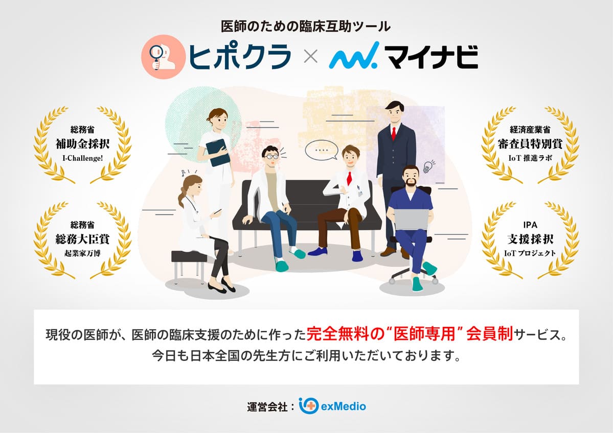
医師のための臨床サポートサービス
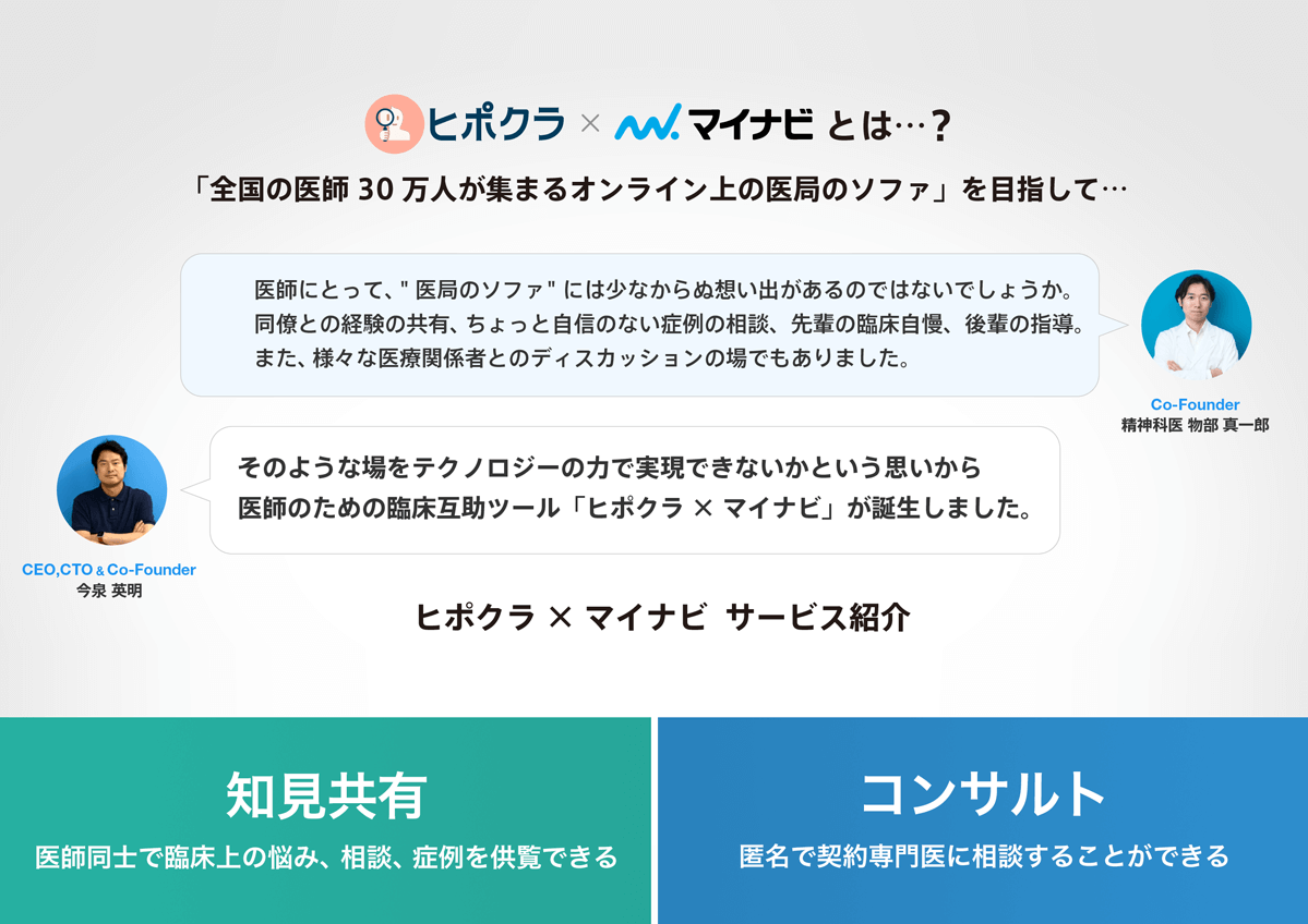
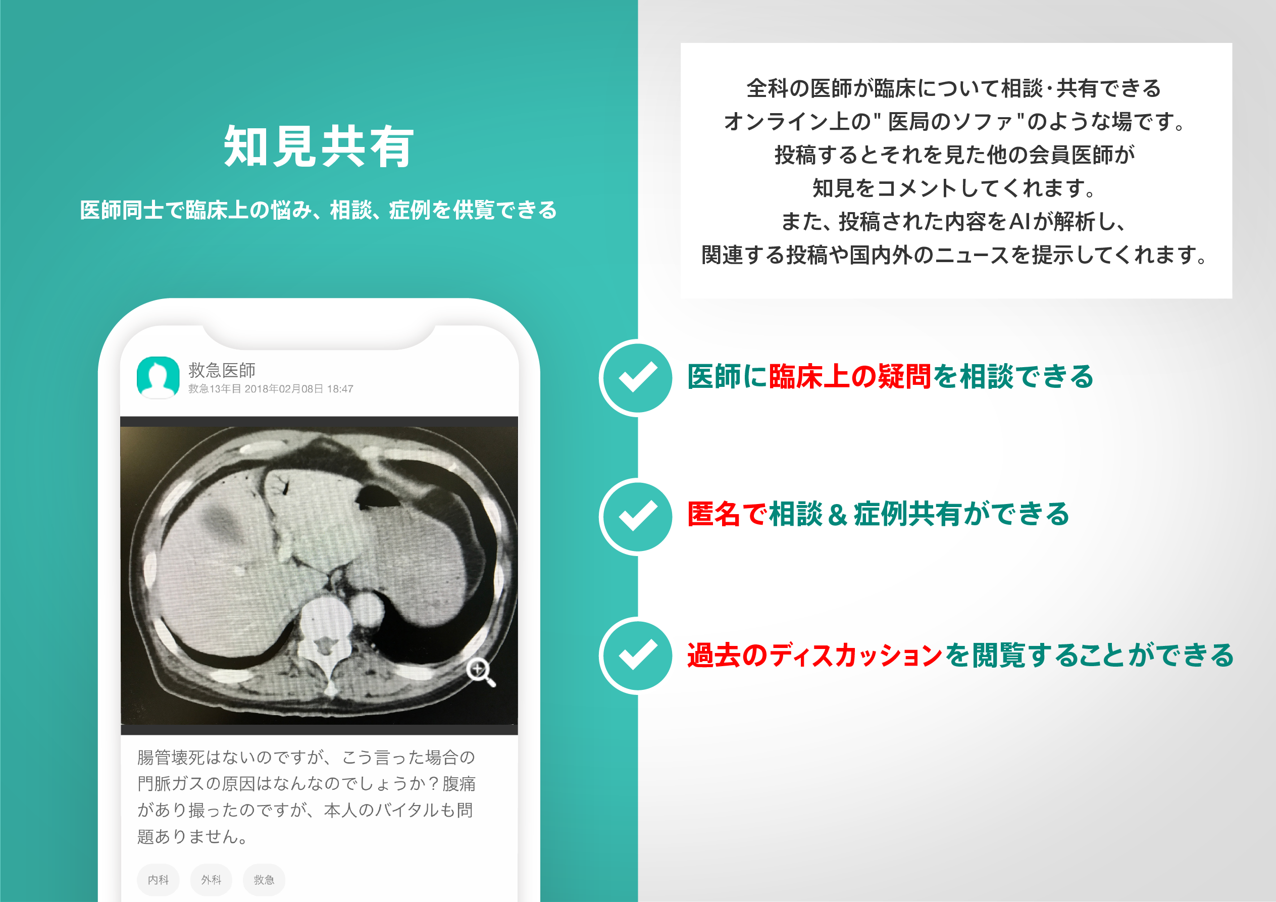
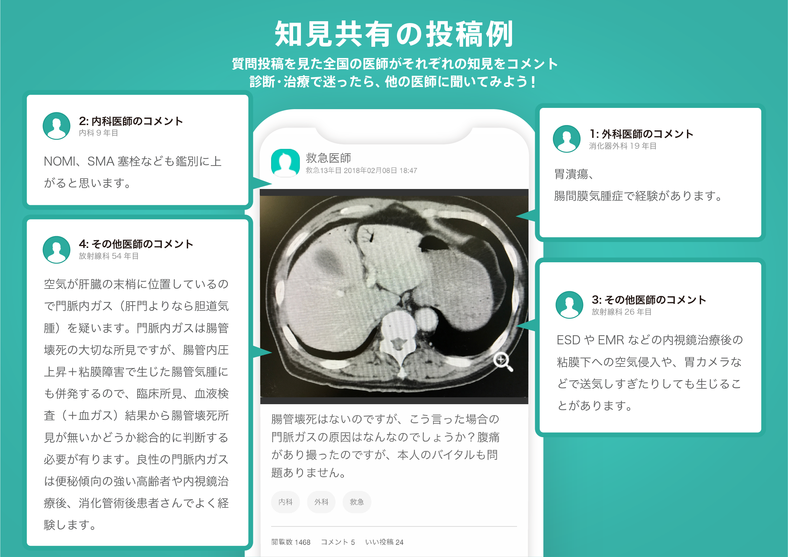
ヒポクラ x マイナビのご紹介
無料会員登録していただくと、さらに便利で効率的な検索が可能になります。