著名医師による解説が無料で読めます
すると翻訳の精度が向上します
プラズモニック導波路の製造などの用途向けに、集中した電子ビームを使用して基板上のナノ粒子の配列を製造するパターニング技術を開発しました(Noriki、T。; Abe、s。;。Kajikawa、K。; Shimojo、M。BeilsteinJ。この手法は3つのステップで構成されています。まず、ナノ粒子は基質の表面全体に配置されます。第二に、ナノ粒子は、焦点を合わせた電子ビーム照射によって基質上に固定されます。電子ビームは、粒子の周りにある有機分子をアモルファス炭素に分解します。アモルファス炭素は、基板上の粒子を固定します。最後に、固定されていないナノ粒子が除去されます。ただし、この元の手法では、ナノ粒子が固定された領域は、数ナノメートルの電子プローブサイズよりも広かった。この拡大メカニズムを理解するために、実験とシミュレーションの両方によって、電圧、粒子サイズ、および基質材料の加速の効果が調査されます。固定領域は、基質によって逆散乱された電子によって大きく影響を受けることが実証されています。バックスカタリングは、ライン幅の増加につながり、したがってこのパターニング手法の解像度を減らします。
プラズモニック導波路の製造などの用途向けに、集中した電子ビームを使用して基板上のナノ粒子の配列を製造するパターニング技術を開発しました(Noriki、T。; Abe、s。;。Kajikawa、K。; Shimojo、M。BeilsteinJ。この手法は3つのステップで構成されています。まず、ナノ粒子は基質の表面全体に配置されます。第二に、ナノ粒子は、焦点を合わせた電子ビーム照射によって基質上に固定されます。電子ビームは、粒子の周りにある有機分子をアモルファス炭素に分解します。アモルファス炭素は、基板上の粒子を固定します。最後に、固定されていないナノ粒子が除去されます。ただし、この元の手法では、ナノ粒子が固定された領域は、数ナノメートルの電子プローブサイズよりも広かった。この拡大メカニズムを理解するために、実験とシミュレーションの両方によって、電圧、粒子サイズ、および基質材料の加速の効果が調査されます。固定領域は、基質によって逆散乱された電子によって大きく影響を受けることが実証されています。バックスカタリングは、ライン幅の増加につながり、したがってこのパターニング手法の解像度を減らします。
For applications such as the fabrication of plasmonic waveguides we developed a patterning technique to fabricate an array of nanoparticles on a substrate using focused electron beams (Noriki, T.; Abe, S.;.Kajikawa, K.; Shimojo, M. Beilstein J. Nanotechnol.2015,6, 1010-1015). This technique consists of three steps: Firstly, nanoparticles are placed over the entire surface of a substrate. Secondly, the nanoparticles are fixed on the substrate by focused electron beam irradiation. The electron beam decomposes the organic molecules located around the particle into amorphous carbon. The amorphous carbon immobilizes the particle on the substrate. Finally, the unfixed nanoparticles are removed. However, in this original technique, the area in which the nanoparticles were fixed was wider than the electron-probe size of a few nanometers. To understand this widening mechanisms, the effects of accelerating voltage, particle size and substrate material are investigated by means of both experiments and simulation. It is demonstrated that the fixing area is greatly affected by the electrons back-scattered by the substrate. The back-scattering leads to an increase in line width and thus reduces the resolution of this patterning technique.
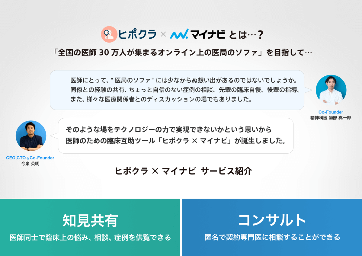
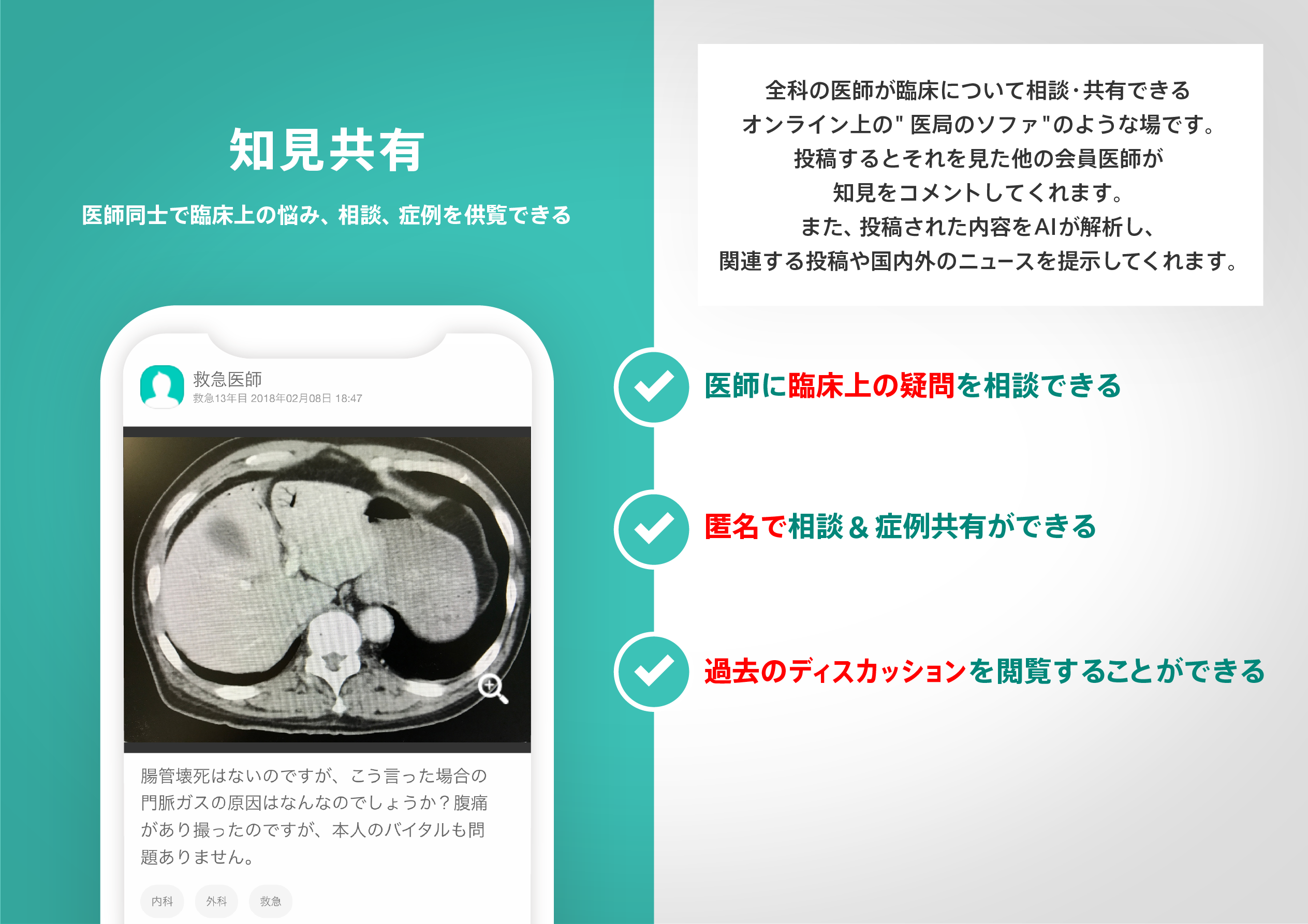
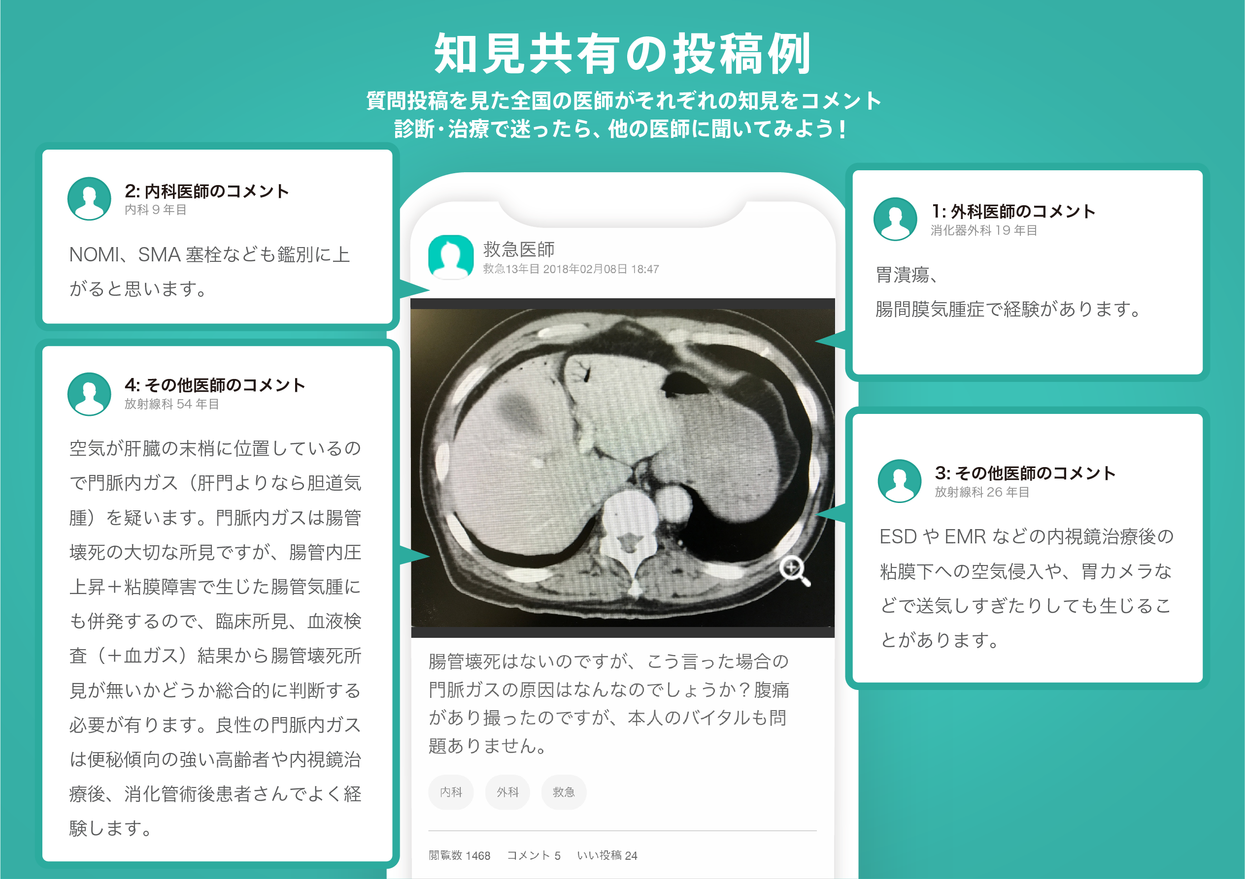
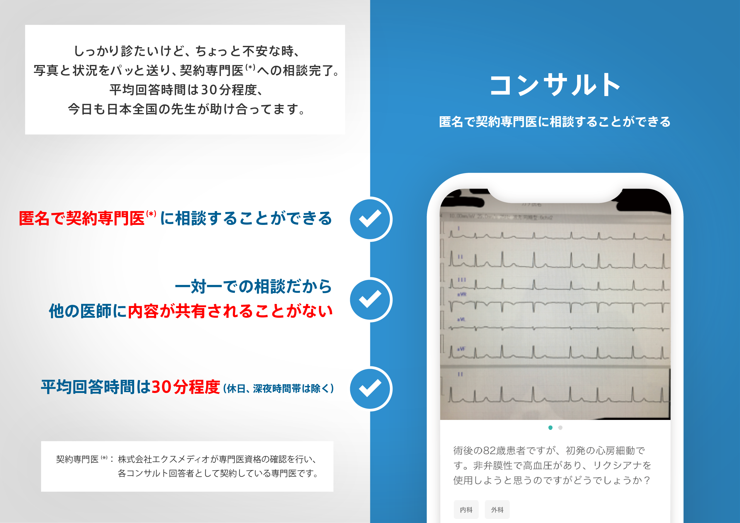
医師のための臨床サポートサービス
ヒポクラ x マイナビのご紹介

無料会員登録していただくと、さらに便利で効率的な検索が可能になります。