著名医師による解説が無料で読めます
すると翻訳の精度が向上します
この論文では、異なる表面上の分子ビームエピタキシー(MBE)の方法におけるゲルマニウム - シリコン量子ドットの形成と成長の理論モデリングが実行されます。結晶構成の向き(100)と(111)のシリコン基質が考慮されます。ゲルマニウムシリコンティンシステムは現代のナノおよびオプトエレクトロニクスにとって非常に重要であるため、スズで覆われたシリコン表面の量子ドットの成長の問題に特に注意が払われます。高速トランジスタ。MBE中のこのような半導体化合物の成長プロセスをモデル化するための理論的アプローチが提示されています。Stranski-Krastanow成長モードの層ごとの核形成段階と島の両方の核生成段階について説明します。湿潤層から島への原子の遷移中の自由エネルギーの変化、核形成の活性化障壁、2Dから3D遷移の臨界厚、およびこれらのシステムの量子ドットの表面密度とサイズ分布関数は、確立されたモデルのヘルプ。すべての理論的憶測は、これらの材料の可能なデバイスアプリケーションを念頭に置いて実行されます。特に、GE堆積の基質としてTINで覆われたSi(100)表面を使用することは、低ノイズ選択量子ドット赤外線写真で可能なアプリケーションの量子ドットアレイのサイズの均一性を増加させるために非常に有望である可能性があることが理論的に示されています。
この論文では、異なる表面上の分子ビームエピタキシー(MBE)の方法におけるゲルマニウム - シリコン量子ドットの形成と成長の理論モデリングが実行されます。結晶構成の向き(100)と(111)のシリコン基質が考慮されます。ゲルマニウムシリコンティンシステムは現代のナノおよびオプトエレクトロニクスにとって非常に重要であるため、スズで覆われたシリコン表面の量子ドットの成長の問題に特に注意が払われます。高速トランジスタ。MBE中のこのような半導体化合物の成長プロセスをモデル化するための理論的アプローチが提示されています。Stranski-Krastanow成長モードの層ごとの核形成段階と島の両方の核生成段階について説明します。湿潤層から島への原子の遷移中の自由エネルギーの変化、核形成の活性化障壁、2Dから3D遷移の臨界厚、およびこれらのシステムの量子ドットの表面密度とサイズ分布関数は、確立されたモデルのヘルプ。すべての理論的憶測は、これらの材料の可能なデバイスアプリケーションを念頭に置いて実行されます。特に、GE堆積の基質としてTINで覆われたSi(100)表面を使用することは、低ノイズ選択量子ドット赤外線写真で可能なアプリケーションの量子ドットアレイのサイズの均一性を増加させるために非常に有望である可能性があることが理論的に示されています。
In this paper theoretical modeling of formation and growth of germanium-silicon quantum dots in the method of molecular beam epitaxy (MBE) on different surfaces is carried out. Silicon substrates with crystallographic orientations (100) and (111) are considered. Special attention is paid to the question of growth of quantum dots on the silicon surface covered by tin, since germanium-silicon-tin system is extremely important for contemporary nano- and optoelectronics: for creation of photodetectors, solar cells, light-emitting diodes, and fast-speed transistors. A theoretical approach for modeling growth processes of such semiconductor compounds during the MBE is presented. Both layer-by-layer and island nucleation stages in the Stranski-Krastanow growth mode are described. A change in free energy during transition of atoms from the wetting layer to an island, activation barrier of the nucleation, critical thickness of 2D to 3D transition, as well as surface density and size distribution function of quantum dots in these systems are calculated with the help of the established model. All the theoretical speculations are carried out keeping in mind possible device applications of these materials. In particular, it is theoretically shown that using of the Si(100) surface covered by tin as a substrate for Ge deposition may be very promising for increasing size homogeneity of quantum dot array for possible applications in low-noise selective quantum dot infrared photodetectors.
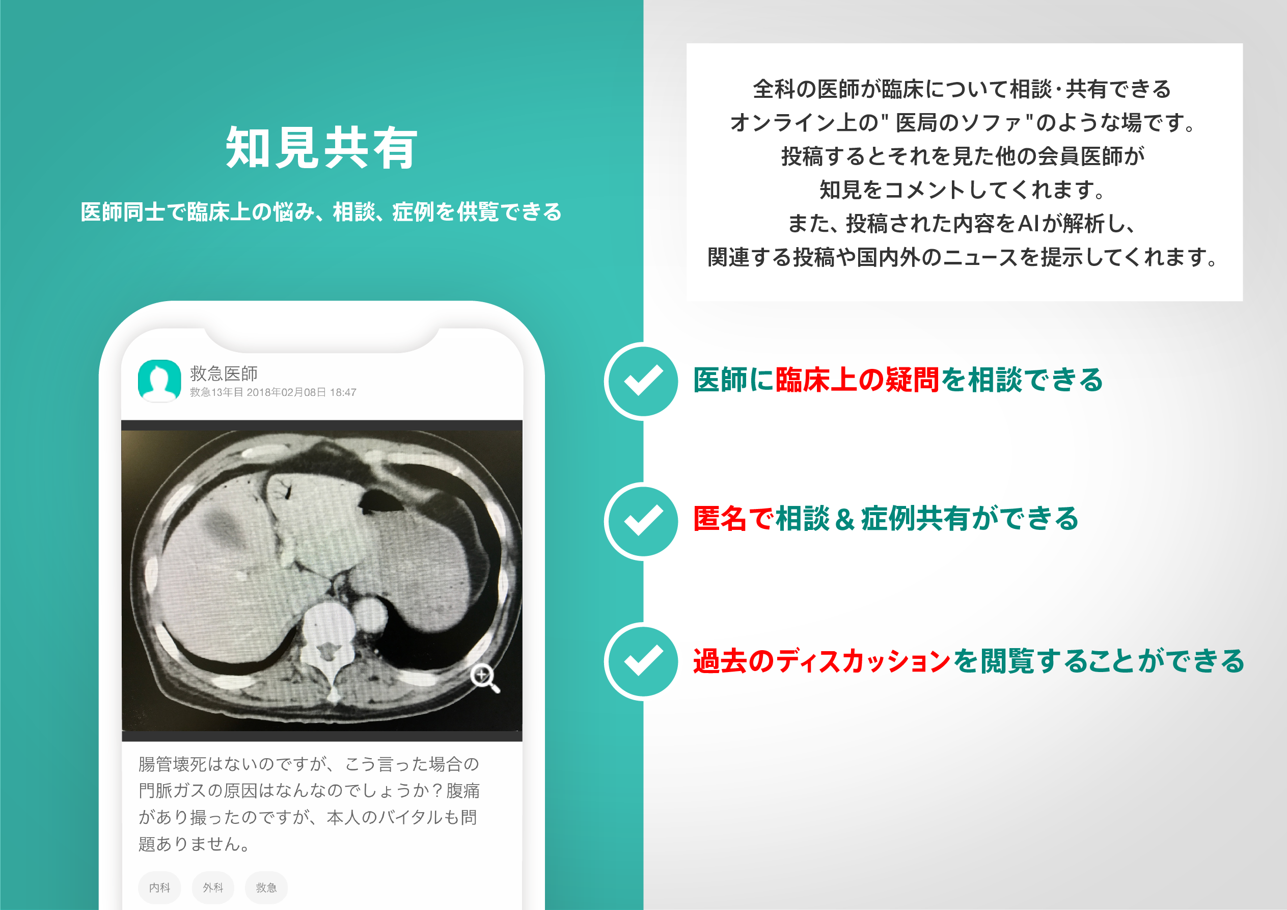
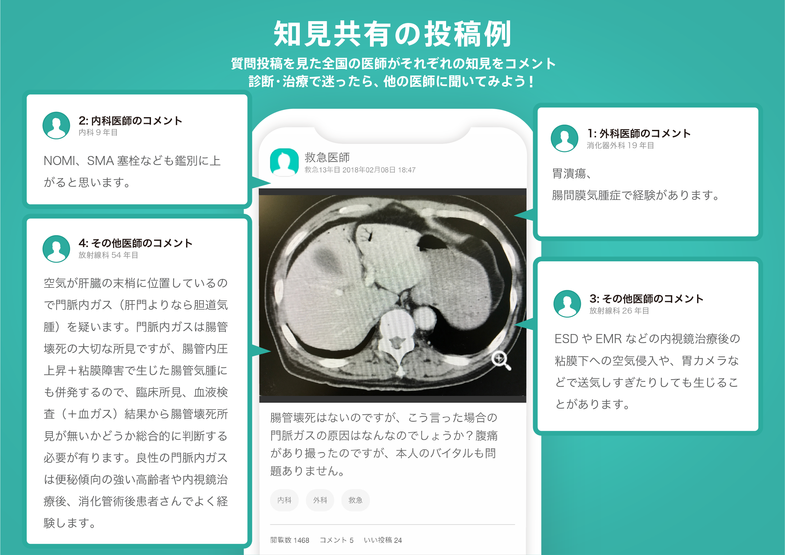
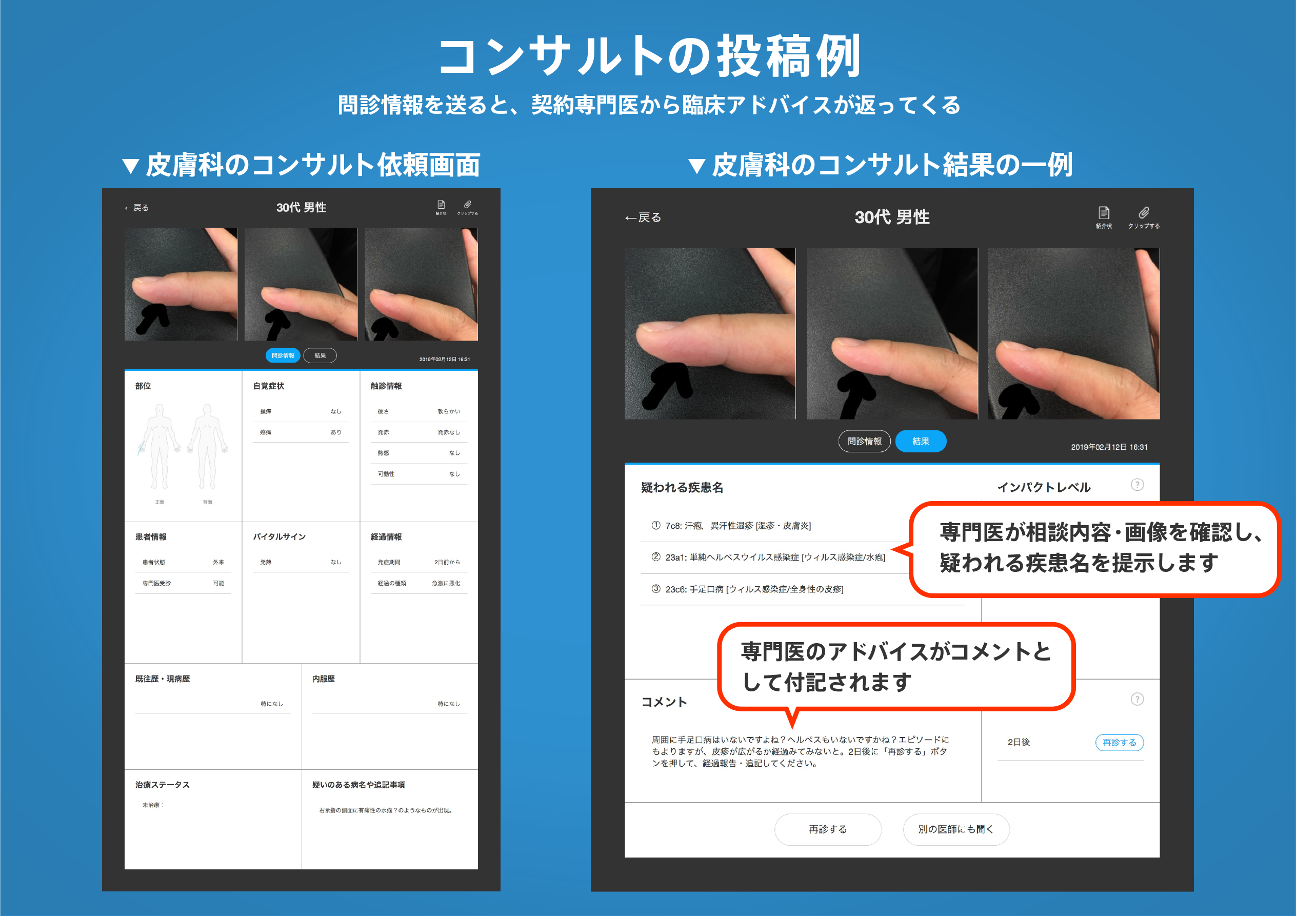
医師のための臨床サポートサービス
ヒポクラ x マイナビのご紹介


無料会員登録していただくと、さらに便利で効率的な検索が可能になります。