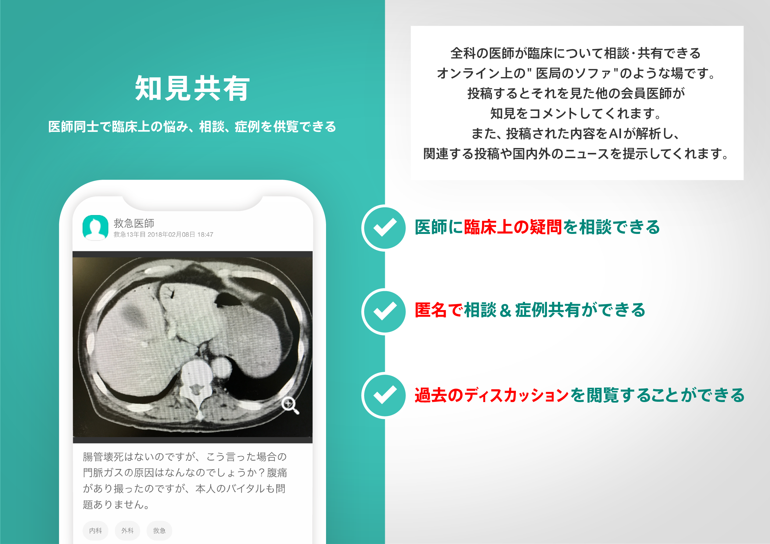
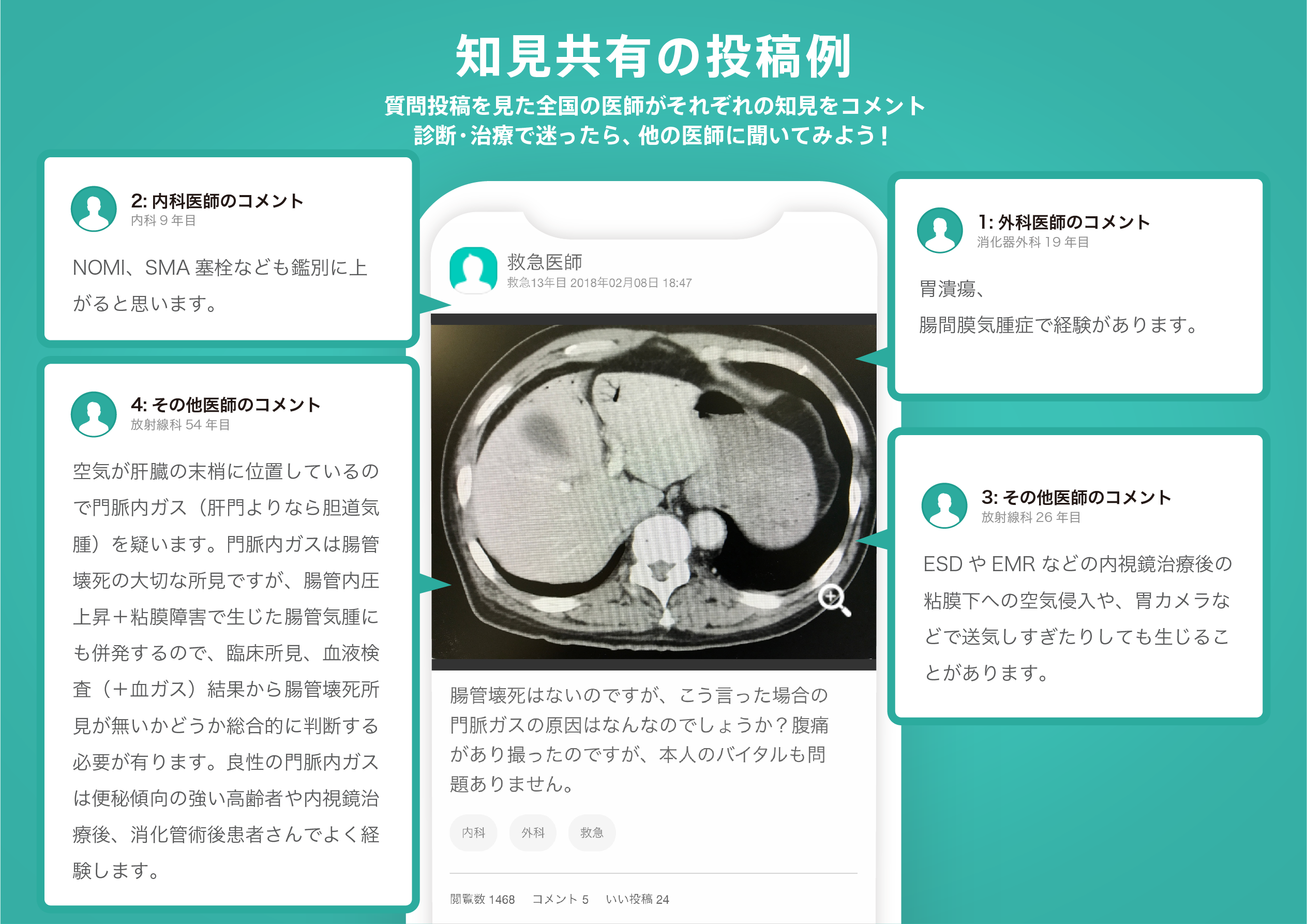
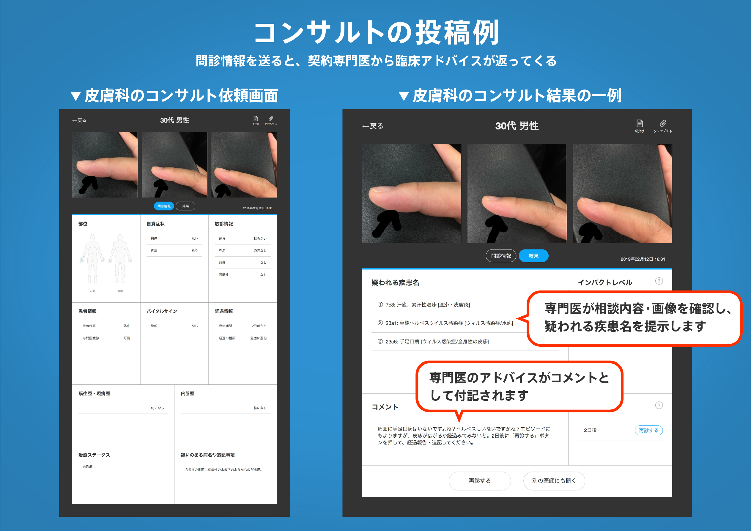
著名医師による解説が無料で読めます
すると翻訳の精度が向上します
ジスルフィドモリブデン(MOS2)は有望なチャネル材料として強調されていますが、MOS2ベースのフィールド効果トランジスタ(FET)は、ゲートインターフェイスの界面トラップから大きな閾値電圧ヒステリシス(ΔVTH)を持っています。この作業では、MOS2 FETSのΔVthは、インターフェイストラップのパッシベーションのためにMOS2/SiO2ゲート界面で3-アミノプロピルトリエトキシシラン(APTES)不動態化層を挿入することにより、大幅に減少します。ΔVthは、ΔVthの主要な供給源である電子のトラッピングとデトラッピングを防ぐため、1%-Paptesのパッシブレイヤーを挿入することにより、23から10.8 Vに減少します。界面トラップ(DIT)の密度の低下は、APTESレイヤーを挿入した後のサブスレッショルドスイング(SS)の改善によって確認されます。さらに、APTESの不動態化を介したMOS2 FETのシナプス特性の改善が調査されています。抑制性および興奮性シナプス後電流(PSC)は、ΔVthの減少とAPTES層のN型ドーピング効果により、33%増加します。さらに、ΔVTHの減少により、シナプス操作がしきい値領域を越えて線形であるため、PSC特性の直線性が大幅に改善されます。APTES Gate Panscivation技術のMOS2 FETSへの適用は、神経型コンピューティングテクノロジーにおける信頼できる正確なシナプスアプリケーションと、次世代の補完論的ロジックアプリケーションに有望です。
ジスルフィドモリブデン(MOS2)は有望なチャネル材料として強調されていますが、MOS2ベースのフィールド効果トランジスタ(FET)は、ゲートインターフェイスの界面トラップから大きな閾値電圧ヒステリシス(ΔVTH)を持っています。この作業では、MOS2 FETSのΔVthは、インターフェイストラップのパッシベーションのためにMOS2/SiO2ゲート界面で3-アミノプロピルトリエトキシシラン(APTES)不動態化層を挿入することにより、大幅に減少します。ΔVthは、ΔVthの主要な供給源である電子のトラッピングとデトラッピングを防ぐため、1%-Paptesのパッシブレイヤーを挿入することにより、23から10.8 Vに減少します。界面トラップ(DIT)の密度の低下は、APTESレイヤーを挿入した後のサブスレッショルドスイング(SS)の改善によって確認されます。さらに、APTESの不動態化を介したMOS2 FETのシナプス特性の改善が調査されています。抑制性および興奮性シナプス後電流(PSC)は、ΔVthの減少とAPTES層のN型ドーピング効果により、33%増加します。さらに、ΔVTHの減少により、シナプス操作がしきい値領域を越えて線形であるため、PSC特性の直線性が大幅に改善されます。APTES Gate Panscivation技術のMOS2 FETSへの適用は、神経型コンピューティングテクノロジーにおける信頼できる正確なシナプスアプリケーションと、次世代の補完論的ロジックアプリケーションに有望です。
Although molybdenum disulfide (MoS2) is highlighted as a promising channel material, MoS2-based field-effect transistors (FETs) have a large threshold voltage hysteresis (Δ VTH) from interface traps at their gate interfaces. In this work, the Δ VTH of MoS2 FETs is significantly reduced by inserting a 3-aminopropyltriethoxysilane (APTES) passivation layer at the MoS2/SiO2 gate interface owing to passivation of the interface traps. The Δ VTH is reduced from 23 to 10.8 V by inserting the 1%-APTES passivation layers because APTES passivation prevents trapping and detrapping of electrons, which are the major source of the Δ VTH. The reduction in the density of interface traps ( Dit) is confirmed by the improvement of the subthreshold swing (SS) after inserting the APTES layer. Furthermore, the improvement in the synaptic characteristics of the MoS2 FET through the APTES passivation is investigated. Both inhibitory and excitatory postsynaptic currents (PSC) are increased by 33% owing to the reduction in the Δ VTH and the n-type doping effect of the APTES layer; moreover, the linearity of PSC characteristics is significantly improved because the reduction in Δ VTH enables the synaptic operation to be over the threshold region, which is linear. The application of the APTES gate passivation technique to MoS2 FETs is promising for reliable and accurate synaptic applications in neuromorphic computing technology as well as for the next-generation complementary logic applications.
医師のための臨床サポートサービス
ヒポクラ x マイナビのご紹介


無料会員登録していただくと、さらに便利で効率的な検索が可能になります。