著名医師による解説が無料で読めます
すると翻訳の精度が向上します
通信システムの複雑さが増えるには、電子機器とフォトニクスの共統合が必要です。しかし、標準的で確立されたシリコンフォトニクスを備えた薄膜niobate(TFLN)エレクトロオプティックモジュレーターの統合に関連するいくつかの課題がまだあります。現在のTFLNプラットフォームは、TFLNの上部にあるシリコン基板の除去や無線周波数(RF)電極の形成など、基板または複雑な製造要件の選択により、シリコンフォトニクス鋳造プロセスとほとんど互換性がありません。ここでは、最初にすべての光学およびRF波動構造が製造されるプラットフォームで報告し、次にTFLNが唯一の追加ステップとしてシリコンフォトチップの上に接着されます。したがって、基質除去の必要性は排除され、TFLN結合の最後のステップを除き、その製造プロセスはシリコンファウンドリー互換であり、他の製造方法と比較してはるかに簡単です。
通信システムの複雑さが増えるには、電子機器とフォトニクスの共統合が必要です。しかし、標準的で確立されたシリコンフォトニクスを備えた薄膜niobate(TFLN)エレクトロオプティックモジュレーターの統合に関連するいくつかの課題がまだあります。現在のTFLNプラットフォームは、TFLNの上部にあるシリコン基板の除去や無線周波数(RF)電極の形成など、基板または複雑な製造要件の選択により、シリコンフォトニクス鋳造プロセスとほとんど互換性がありません。ここでは、最初にすべての光学およびRF波動構造が製造されるプラットフォームで報告し、次にTFLNが唯一の追加ステップとしてシリコンフォトチップの上に接着されます。したがって、基質除去の必要性は排除され、TFLN結合の最後のステップを除き、その製造プロセスはシリコンファウンドリー互換であり、他の製造方法と比較してはるかに簡単です。
Ever-increasing complexity of communication systems demands the co-integration of electronics and photonics. But there are still some challenges associated with the integration of thin film lithium niobate (TFLN) electro-optic modulators with the standard and well-established silicon photonics. Current TFLN platforms are mostly not compatible with the silicon photonics foundry process due to the choice of substrate or complicated fabrication requirements, including silicon substrate removal and formation of radio-frequency (RF) electrodes on the top of the TFLN. Here, we report on a platform where all the optical and RF waveguiding structures are fabricated first, and then the TFLN is bonded on top of the silicon photonic chip as the only additional step. Hence, the need for substrate removal is eliminated, and except for the last step of TFLN bonding, its fabrication process is silicon foundry compatible and much more straightforward compared to other fabrication methods.
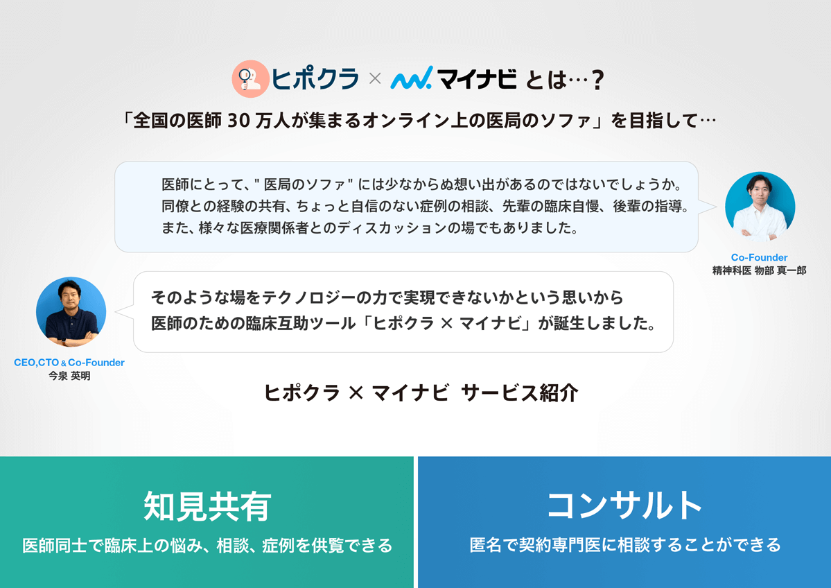
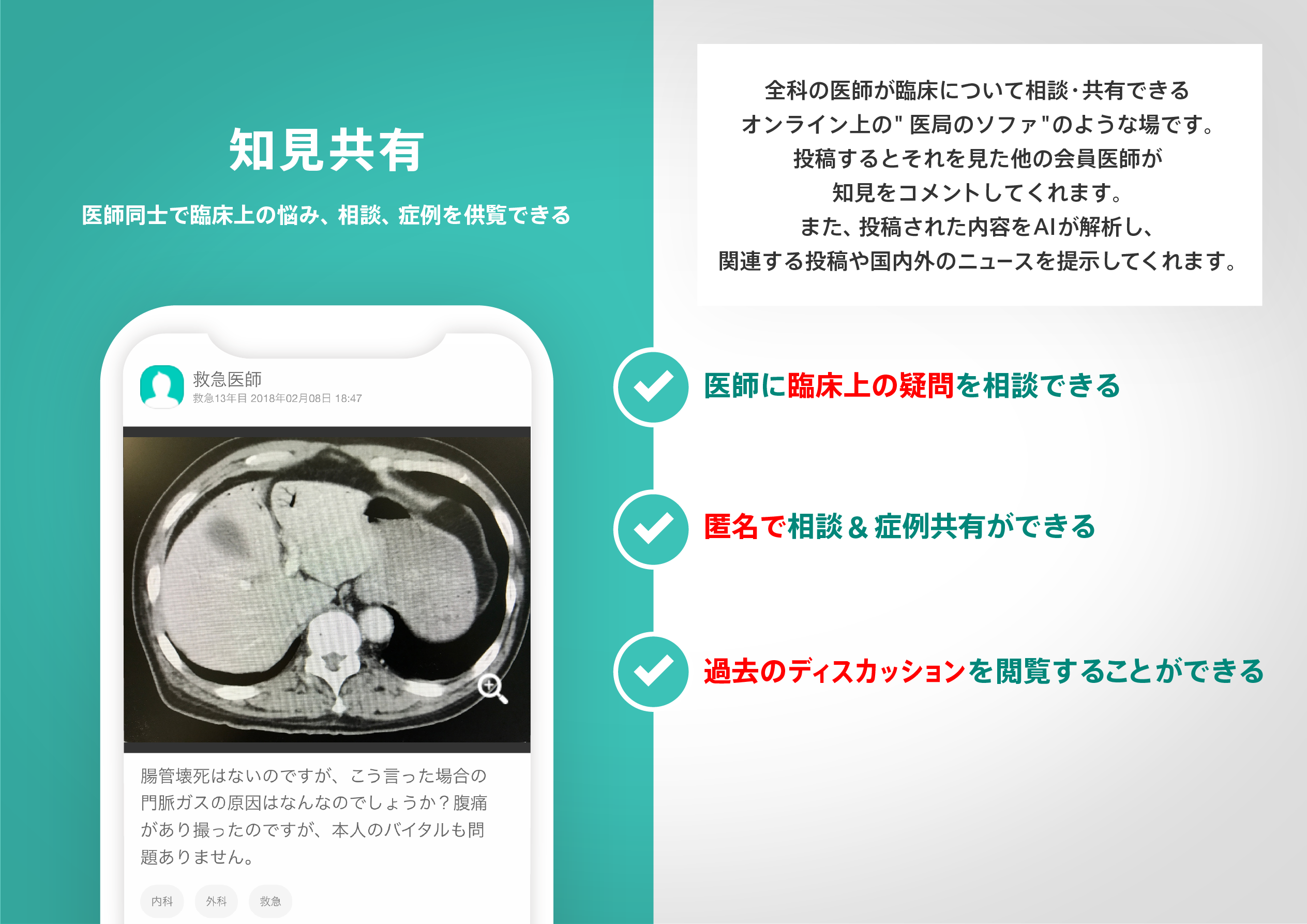
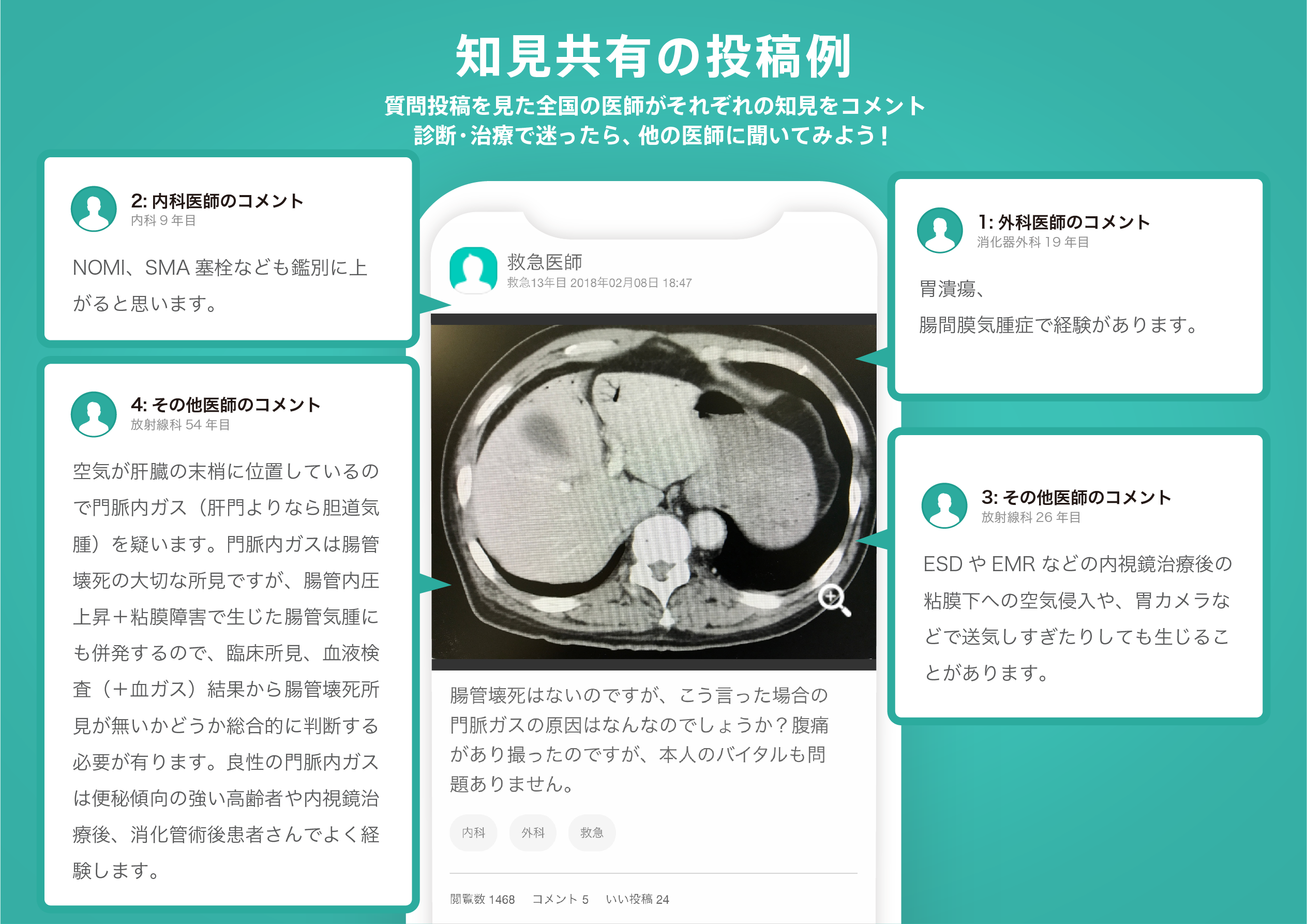
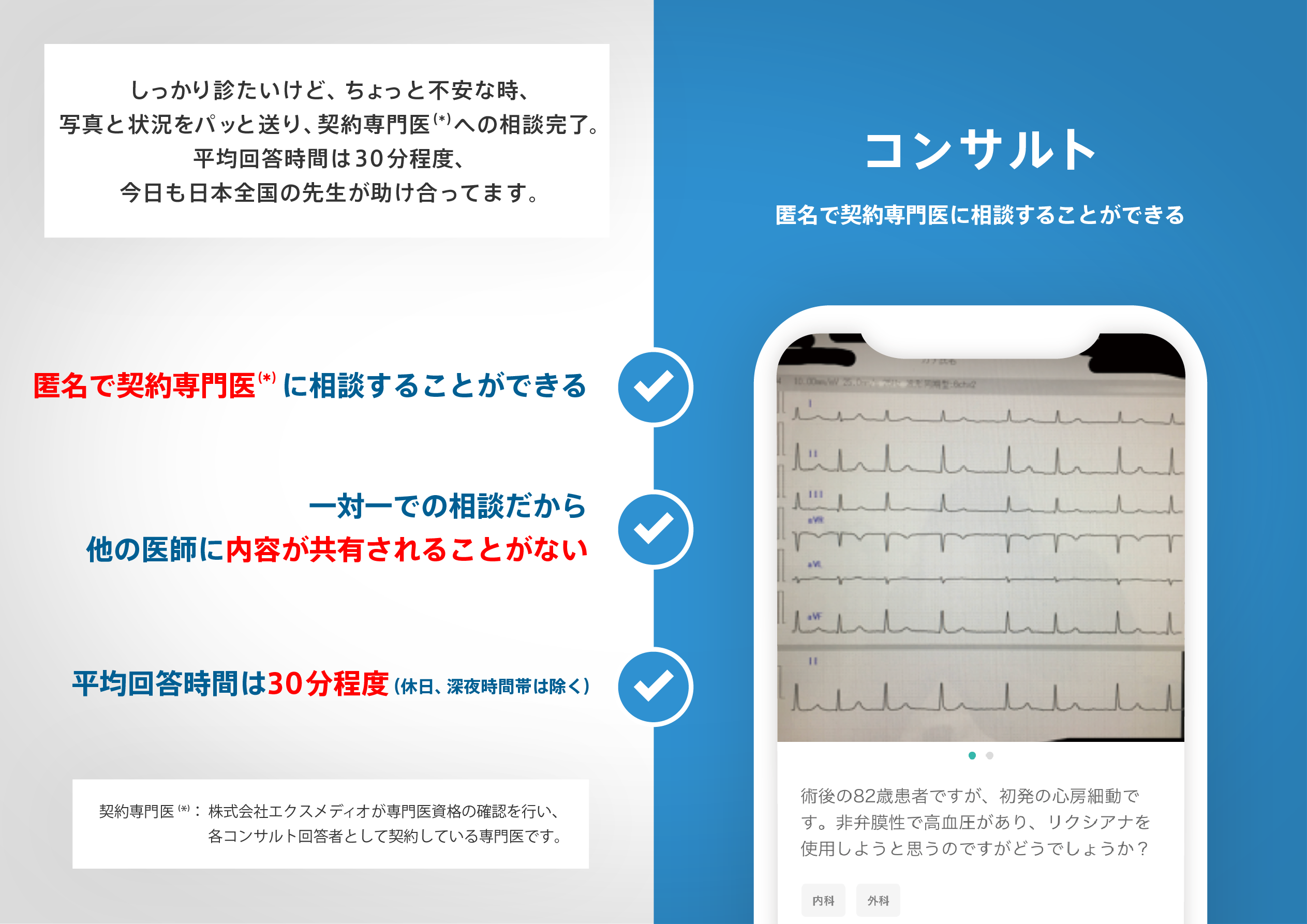
医師のための臨床サポートサービス
ヒポクラ x マイナビのご紹介

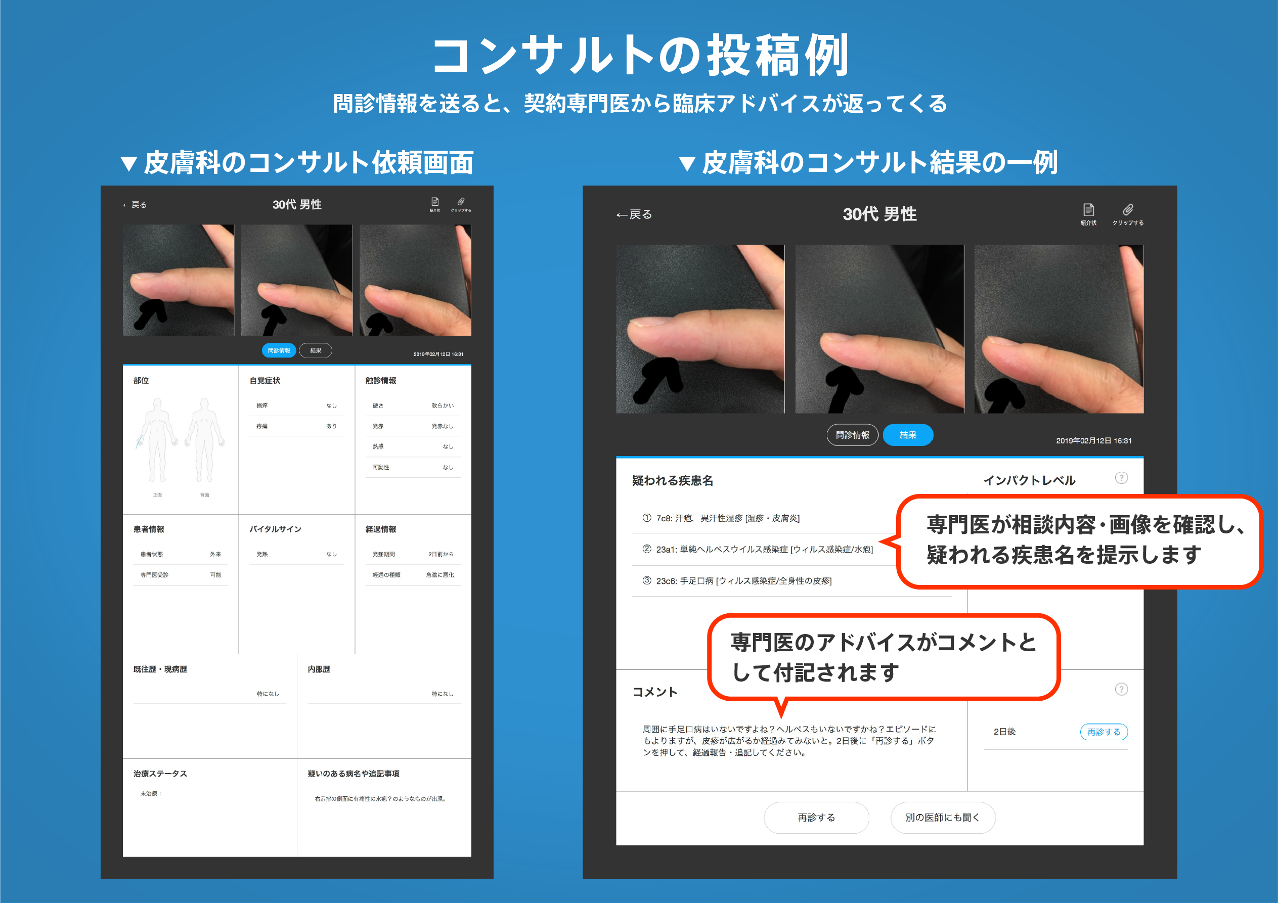
無料会員登録していただくと、さらに便利で効率的な検索が可能になります。