著名医師による解説が無料で読めます
すると翻訳の精度が向上します
ひずみや電界などの外部摂動に対するHFN2単層の電子特性の応答は、そのデバイスベースのアプリケーションと光触媒の密度官能理論計算を使用して広く調査されています。HFN2単層は、1.44 eVの直接バンドギャップを示す半導体であることがわかりました。さらに、±10%の二軸株下で水酸化還元電位にまたがるHFN2単層のエッジのバンドエッジの調整性により、pHの広範囲(0-7)にわたる光触媒アプリケーションを介した太陽エネルギーの収穫に適しています。バンドギャップは、10%の二軸引張株で29.8%減少する可能性があります。スピン軌道カップリング(SOC)が組み込まれると、伝導帯(ΔC〜314 MEV)での大規模なスピン分割と価数帯域での小さな分割(ΔV〜32 MEV)が認められます。エッジ。バンドエッジのスピン分割は、二軸圧縮ひずみによって調整可能であることがわかります。ひずみ依存の機械的特性と安定性は、HFN2単層が最大±10%の大きな株に耐える能力を明らかにし、それにより、若い弾性率(Y)に66 N M-1から283 Nに巨大な調整性をもたらします。M-1。これは、柔軟な電子機器で搾取可能です。このような幅広い範囲でのYの調整性は、他の2D材料では観察されていません。さらに、HFN2単層は、0.48VÅ-1の通常の電界またはゲート電圧の適用下で半導体から金属状態への移行を受けます。デバイス。興味深いことに、このような強度の電界は、パルスACフィールドテクノロジーを使用して実験的に実現されています。このような小さなゲート電圧は、その消費電力を大幅に低下させます。オフからオン状態へのこの移行の電子起源は、空いていないNFEG(ほぼ自由電子ガス)状態から生じることがわかります。HFN2単層ベースのトンネルフィールドエフェクトトランジスタ(T-FET)が、低電力デジタルデータストレージのモデルデバイスとして提案されており、柔軟なエレクトロニクスとメモリデバイスの新しい道を舗装します。
ひずみや電界などの外部摂動に対するHFN2単層の電子特性の応答は、そのデバイスベースのアプリケーションと光触媒の密度官能理論計算を使用して広く調査されています。HFN2単層は、1.44 eVの直接バンドギャップを示す半導体であることがわかりました。さらに、±10%の二軸株下で水酸化還元電位にまたがるHFN2単層のエッジのバンドエッジの調整性により、pHの広範囲(0-7)にわたる光触媒アプリケーションを介した太陽エネルギーの収穫に適しています。バンドギャップは、10%の二軸引張株で29.8%減少する可能性があります。スピン軌道カップリング(SOC)が組み込まれると、伝導帯(ΔC〜314 MEV)での大規模なスピン分割と価数帯域での小さな分割(ΔV〜32 MEV)が認められます。エッジ。バンドエッジのスピン分割は、二軸圧縮ひずみによって調整可能であることがわかります。ひずみ依存の機械的特性と安定性は、HFN2単層が最大±10%の大きな株に耐える能力を明らかにし、それにより、若い弾性率(Y)に66 N M-1から283 Nに巨大な調整性をもたらします。M-1。これは、柔軟な電子機器で搾取可能です。このような幅広い範囲でのYの調整性は、他の2D材料では観察されていません。さらに、HFN2単層は、0.48VÅ-1の通常の電界またはゲート電圧の適用下で半導体から金属状態への移行を受けます。デバイス。興味深いことに、このような強度の電界は、パルスACフィールドテクノロジーを使用して実験的に実現されています。このような小さなゲート電圧は、その消費電力を大幅に低下させます。オフからオン状態へのこの移行の電子起源は、空いていないNFEG(ほぼ自由電子ガス)状態から生じることがわかります。HFN2単層ベースのトンネルフィールドエフェクトトランジスタ(T-FET)が、低電力デジタルデータストレージのモデルデバイスとして提案されており、柔軟なエレクトロニクスとメモリデバイスの新しい道を舗装します。
The response of the electronic properties of the HfN2 monolayer to external perturbation, such as strain and electric fields, has been extensively investigated using density functional theory calculations for its device-based applications and photocatalysis. The HfN2 monolayer is found to be a semiconductor showing a direct band gap of 1.44 eV, which is widely tunable by 0.9 eV via application of biaxial strain. Furthermore, the tunability in the band edges of the HfN2 monolayer straddling the water redox potential under a biaxial strain of ±10% makes it suitable for solar energy harvesting via photocatalytic applications over a wide range (0-7) of pH. The band gap can be decreased by 29.8% under a biaxial tensile strain of 10%. Upon incorporation of spin orbit coupling (SOC) a large spin splitting at the conduction band (Δc ∼ 314 meV) and a small splitting at the valence band (Δv ∼ 32 meV) are noted, which is attributable to the orbital composition of the band edges. The spin splitting in the band edges is found to be adjustable via biaxial compressive strain. The strain dependent mechanical properties and stability reveal the ability of the HfN2 monolayer to withstand a large magnitude of strain of up to ±10%, thereby bringing about a giant tunability in its Young modulus (Y) from 66 N m-1 to 283 N m-1, which is gainfully exploitable in flexible electronics. The tunability in Y over such a wide range has not been observed in other 2D materials. Moreover, the HfN2 monolayer undergoes a transition from a semiconducting to a metallic state under the application of a normal electric field or gate voltage of 0.48 V Å-1, which may potentially serve as the OFF (semiconducting) and ON (metallic) state in devices. Interestingly, an electric field of such intensity has been realized experimentally using pulsed ac field technology. Such a small gate voltage will greatly lower its power consumption. The electronic origin of this transition from the OFF to the ON state is found to arise from unoccupied NFEG (Nearly Free Electron Gas) states. A HfN2 monolayer based tunnel field effect transistor (t-FET) is proposed herewith as a model device for low-power digital data storage, thereby paving new avenues in flexible electronics and memory devices.
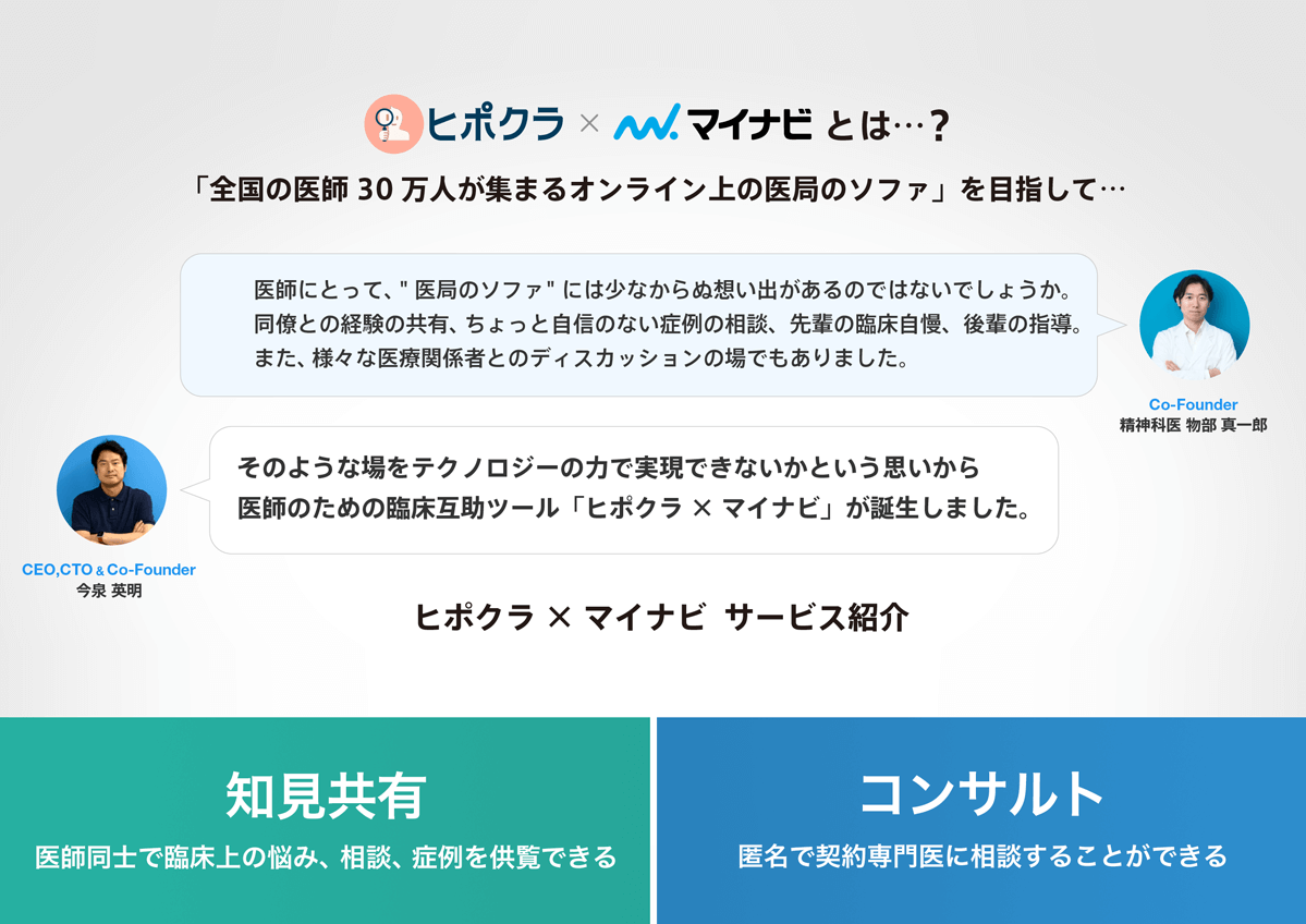
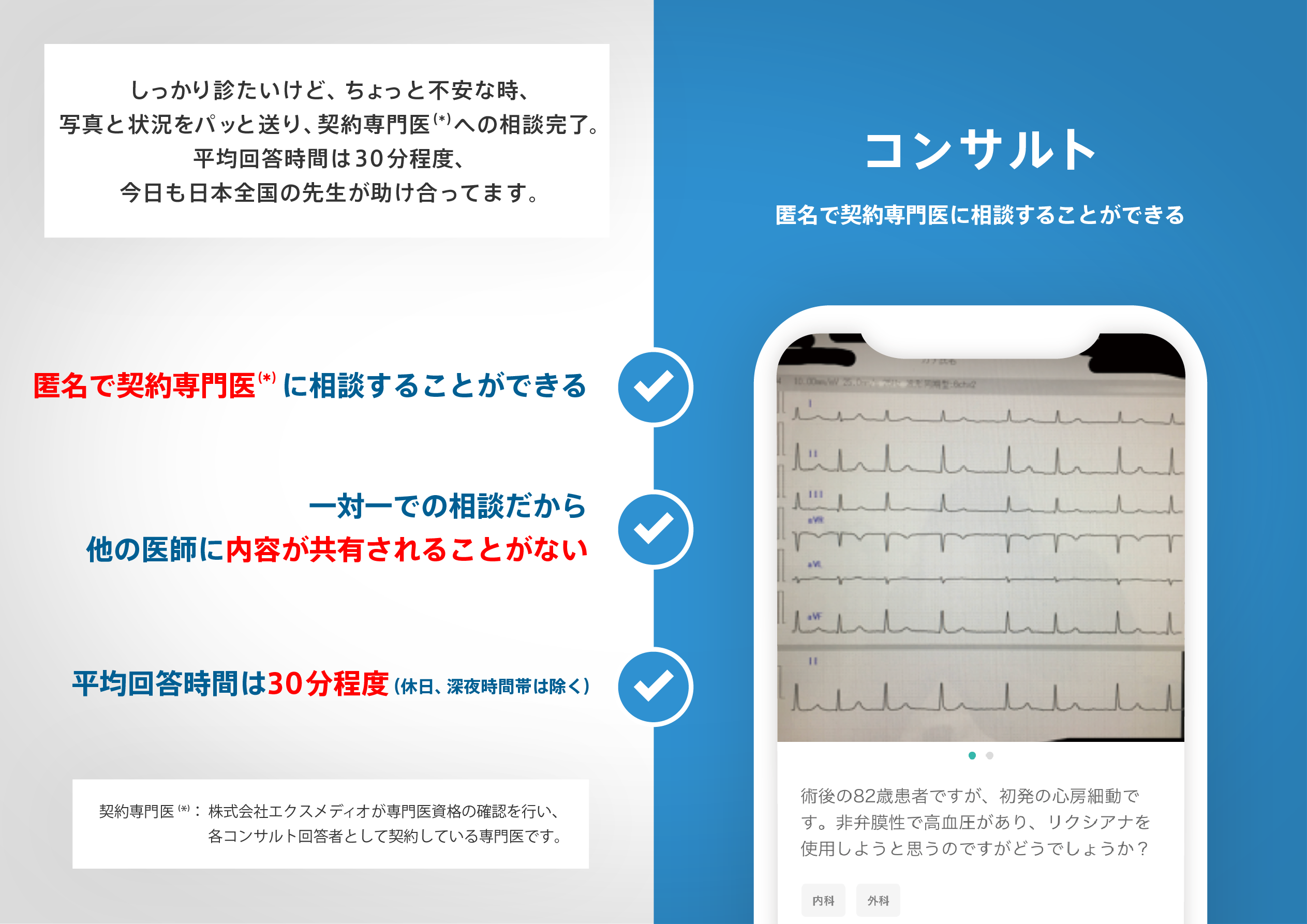
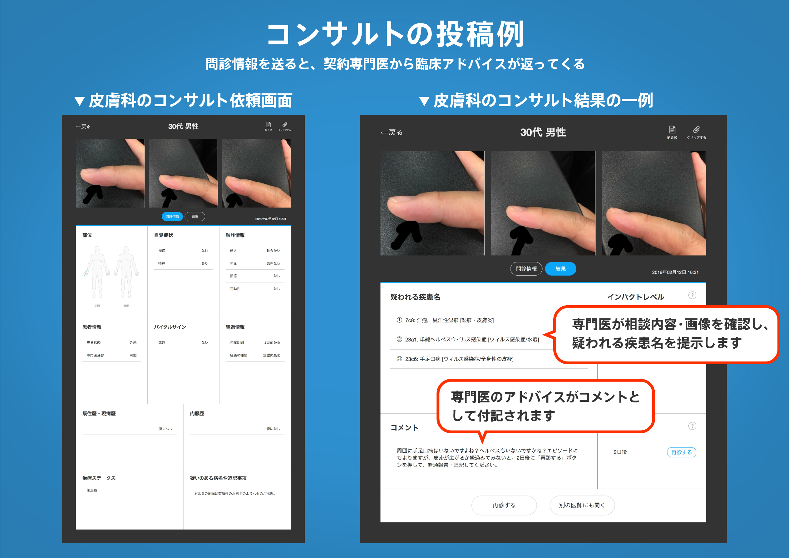
医師のための臨床サポートサービス
ヒポクラ x マイナビのご紹介


無料会員登録していただくと、さらに便利で効率的な検索が可能になります。