著名医師による解説が無料で読めます
すると翻訳の精度が向上します
半導体デバイスの履歴では、この傾向に続いてダイオード、トランジスタ、サイリスタ、および超格子を使用して、材料層の数を絞り込んで増加させると、デバイスの機能を改善する傾向が観察されます。スーパーラティスはユニークな機能を約束しますが、技術の障壁のために広く採用されていないため、分子ビームエピタキシーや格子型材料などの高度な製造が必要です。ここでは、アモルファス材料と物理的蒸気堆積を使用して量子デバイスを設計する方法が提示されています。乗算ゲインmは、n、n、m = knの層の数に依存し、kは乗算の効率を示す因子として依存することが示されています。ただし、このMは輸送時間とのトレードオフであり、これはNにも依存します。実証するために、SiとAS2SE3の超格子とともに光検出器デバイスがSiで製造され、電流ボルテージ(I-V)および電流時間(I-T)測定を使用して特徴付けられます。総層の厚さ200 nmと2μmの超格子の場合、結果はK200NM = 0.916およびK2μm= 0.384であることを示しています。結果は、乗算係数が超格子層の数に関連していることを確認し、設計アプローチの有効性を示しています。
半導体デバイスの履歴では、この傾向に続いてダイオード、トランジスタ、サイリスタ、および超格子を使用して、材料層の数を絞り込んで増加させると、デバイスの機能を改善する傾向が観察されます。スーパーラティスはユニークな機能を約束しますが、技術の障壁のために広く採用されていないため、分子ビームエピタキシーや格子型材料などの高度な製造が必要です。ここでは、アモルファス材料と物理的蒸気堆積を使用して量子デバイスを設計する方法が提示されています。乗算ゲインmは、n、n、m = knの層の数に依存し、kは乗算の効率を示す因子として依存することが示されています。ただし、このMは輸送時間とのトレードオフであり、これはNにも依存します。実証するために、SiとAS2SE3の超格子とともに光検出器デバイスがSiで製造され、電流ボルテージ(I-V)および電流時間(I-T)測定を使用して特徴付けられます。総層の厚さ200 nmと2μmの超格子の場合、結果はK200NM = 0.916およびK2μm= 0.384であることを示しています。結果は、乗算係数が超格子層の数に関連していることを確認し、設計アプローチの有効性を示しています。
In semiconductor device history, a trend is observed where narrowing and increasing the number of material layers improve device functionality, with diodes, transistors, thyristors, and superlattices following this trend. While superlattices promise unique functionality, they are not widely adopted due to a technology barrier, requiring advanced fabrication, such as molecular beam epitaxy and lattice-matched materials. Here, a method to design quantum devices using amorphous materials and physical vapor deposition is presented. It is shown that the multiplication gain M depends on the number of layers of the superlattice, N, as M = kN, with k as a factor indicating the efficiency of multiplication. This M is, however, a trade-off with transit time, which also depends on N. To demonstrate, photodetector devices are fabricated on Si, with the superlattice of Se and As2Se3, and characterized using current-voltage (I-V) and current-time (I-T) measurements. For superlattices with the total layer thicknesses of 200 nm and 2 μm, the results show that k200nm = 0.916 and k2μm = 0.384, respectively. The results confirm that the multiplication factor is related to the number of superlattice layers, showing the effectiveness of the design approach.
医師のための臨床サポートサービス
ヒポクラ x マイナビのご紹介


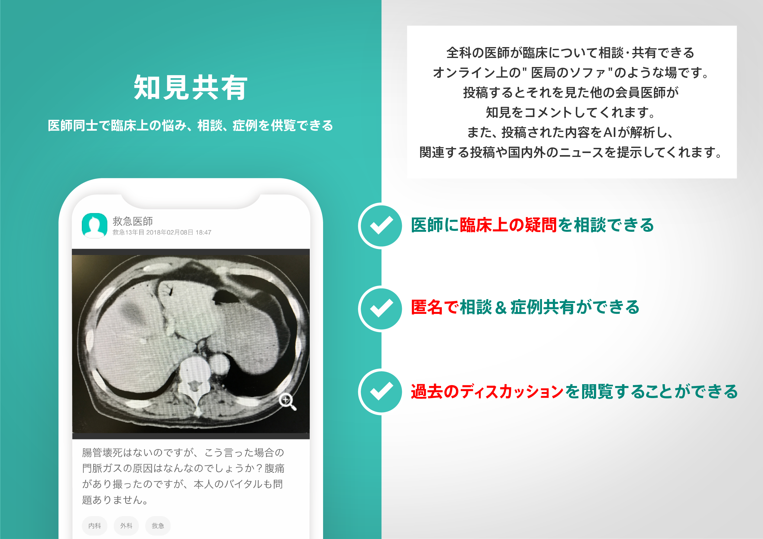
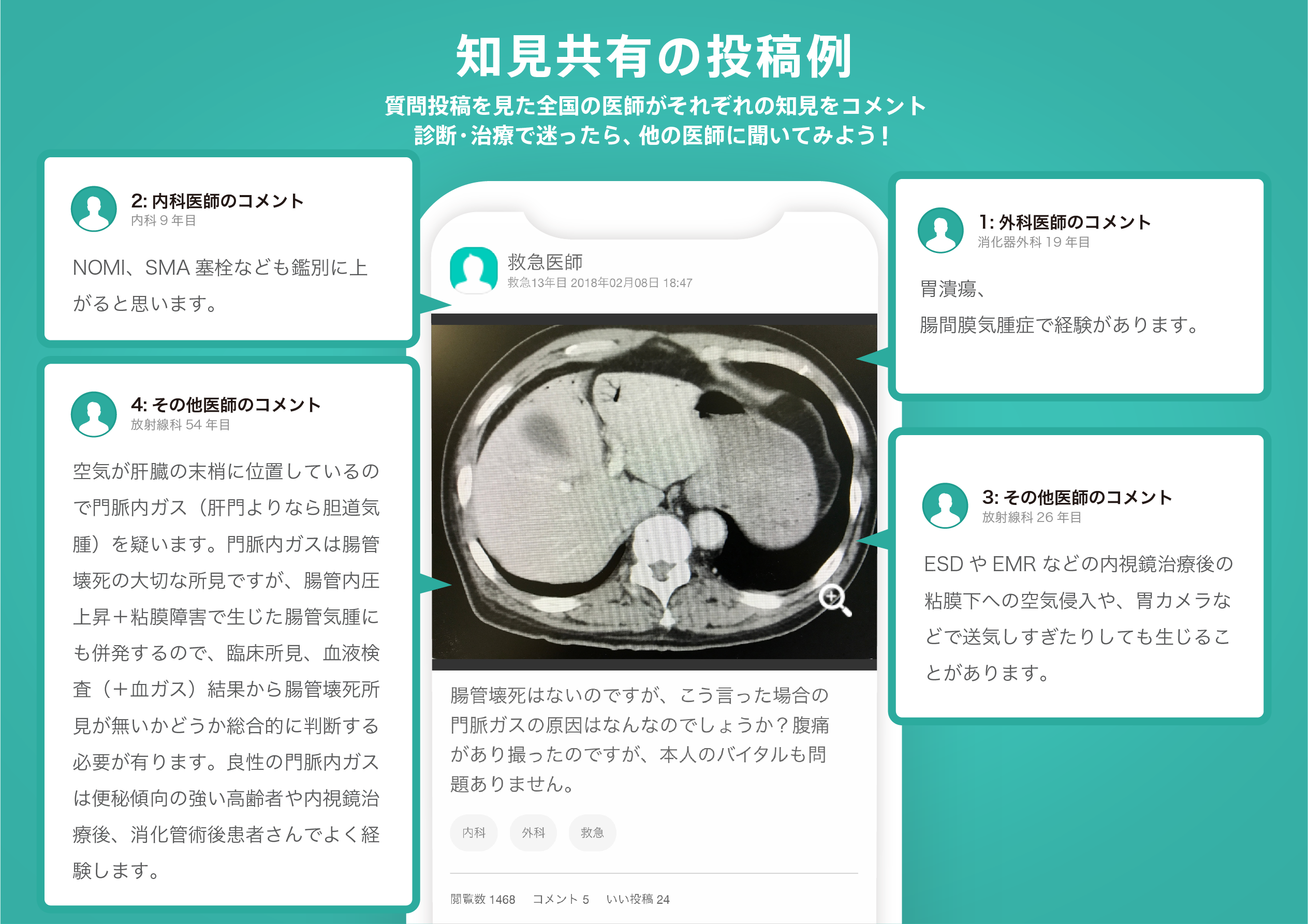
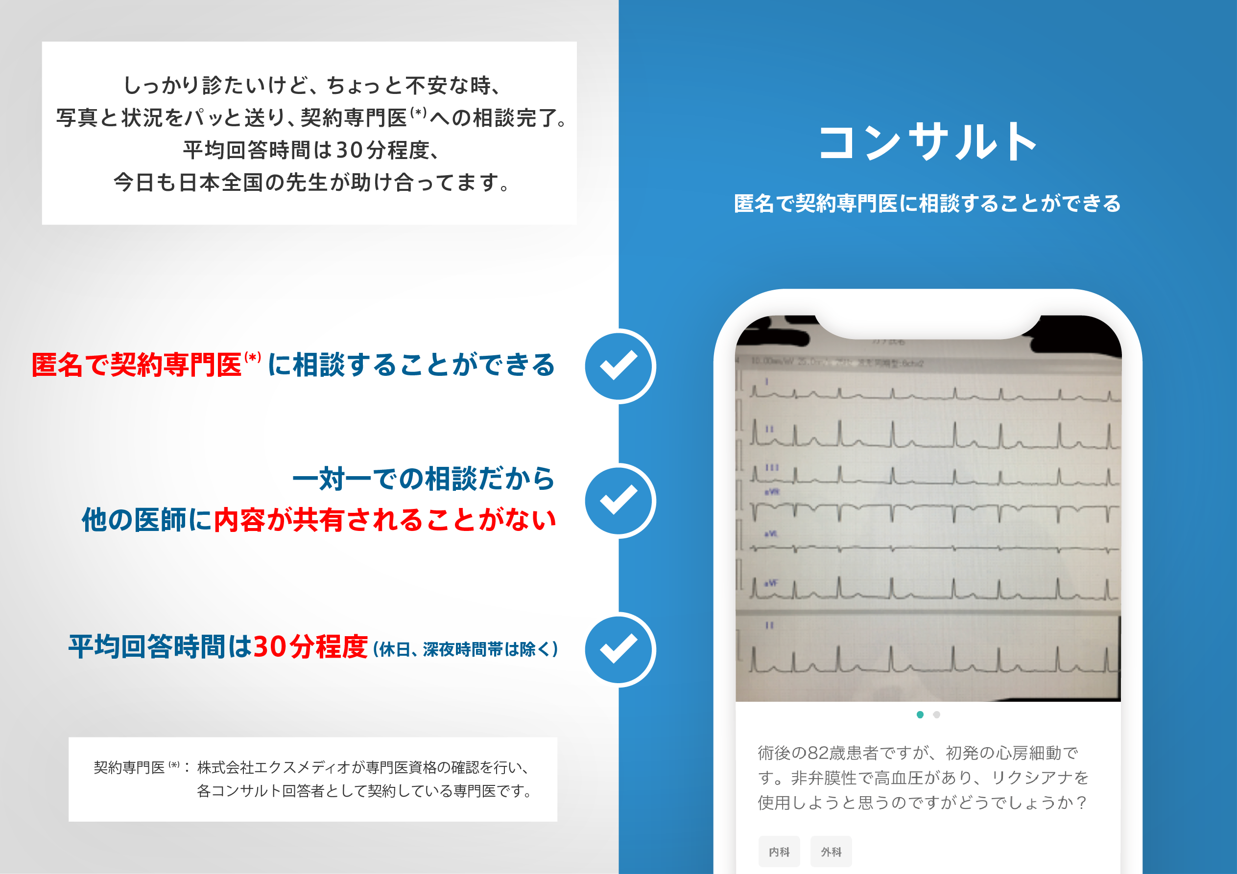
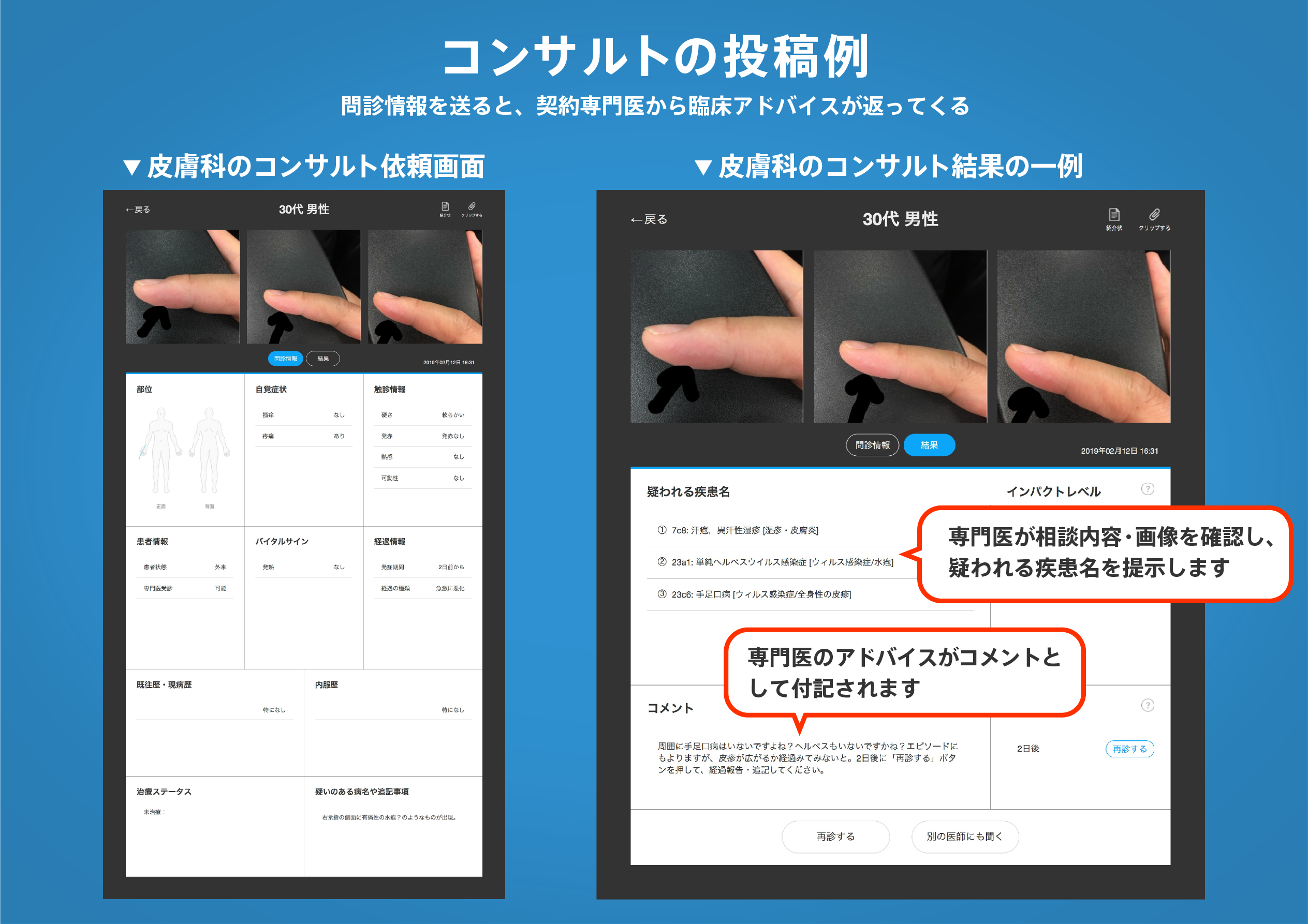
無料会員登録していただくと、さらに便利で効率的な検索が可能になります。