著名医師による解説が無料で読めます
すると翻訳の精度が向上します
sige/si仮想基板上で成長し、2つの静電的に定義されたホールスピンqubitsをホストする緊張したge量子ウェルは、シンクロトロンベースのスキャンX線回折顕微鏡検査によって非破壊的に調査され、そのすべてのbravais格子パラメーターを決定します。これにより、6つのひずみテンソル成分の3次元空間依存性を、横方向の解像度で約50 nmにすることができます。それぞれ<100 nmおよび>1μmで、キュビットの近接でひずみフィールドの変動を支配する2つの異なる空間スケールが観察されます。短いレンジの変動は、典型的な帯域幅2×10⁻⁴であり、キッツを定義する金属電極の圧縮応力作用に定量的にリンクできます。有限要素の機械的シミュレーションにより、このひずみの変動は極低温で最大6×10⁻⁴に増加すると推定されています。長距離の変動は10〜3順序であり、塑性リラックスした仮想基板の不適合転位に関連しています。このことから、それぞれ電極と脱臼について、それぞれ100μEVおよび1 MEVのオーダーの光および重いエネルギーの最大値のエネルギー変動が計算されます。材料関連の不均一性に関するこれらの洞察は、主流のSIベースのマイクロエレクトロニクステクノロジーを使用して製造された大規模な量子プロセッサの最適化と設計のために、さらなるモデリングにフィードルする可能性があります。
sige/si仮想基板上で成長し、2つの静電的に定義されたホールスピンqubitsをホストする緊張したge量子ウェルは、シンクロトロンベースのスキャンX線回折顕微鏡検査によって非破壊的に調査され、そのすべてのbravais格子パラメーターを決定します。これにより、6つのひずみテンソル成分の3次元空間依存性を、横方向の解像度で約50 nmにすることができます。それぞれ<100 nmおよび>1μmで、キュビットの近接でひずみフィールドの変動を支配する2つの異なる空間スケールが観察されます。短いレンジの変動は、典型的な帯域幅2×10⁻⁴であり、キッツを定義する金属電極の圧縮応力作用に定量的にリンクできます。有限要素の機械的シミュレーションにより、このひずみの変動は極低温で最大6×10⁻⁴に増加すると推定されています。長距離の変動は10〜3順序であり、塑性リラックスした仮想基板の不適合転位に関連しています。このことから、それぞれ電極と脱臼について、それぞれ100μEVおよび1 MEVのオーダーの光および重いエネルギーの最大値のエネルギー変動が計算されます。材料関連の不均一性に関するこれらの洞察は、主流のSIベースのマイクロエレクトロニクステクノロジーを使用して製造された大規模な量子プロセッサの最適化と設計のために、さらなるモデリングにフィードルする可能性があります。
A strained Ge quantum well, grown on a SiGe/Si virtual substrate and hosting two electrostatically defined hole spin qubits, is nondestructively investigated by synchrotron-based scanning X-ray diffraction microscopy to determine all its Bravais lattice parameters. This allows rendering the three-dimensional spatial dependence of the six strain tensor components with a lateral resolution of approximately 50 nm. Two different spatial scales governing the strain field fluctuations in proximity of the qubits are observed at <100 nm and >1 μm, respectively. The short-ranged fluctuations have a typical bandwidth of 2 × 10⁻⁴ and can be quantitatively linked to the compressive stressing action of the metal electrodes defining the qubits. By finite element mechanical simulations, it is estimated that this strain fluctuation is increased up to 6 × 10⁻⁴ at cryogenic temperature. The longer-ranged fluctuations are of the 10-3 order and are associated with misfit dislocations in the plastically relaxed virtual substrate. From this, energy variations of the light and heavy-hole energy maxima of the order of several 100 μeV and 1 meV are calculated for electrodes and dislocations, respectively. These insights over material-related inhomogeneities may feed into further modeling for optimization and design of large-scale quantum processors manufactured using the mainstream Si-based microelectronics technology.
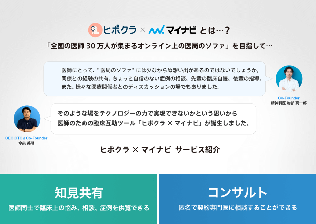
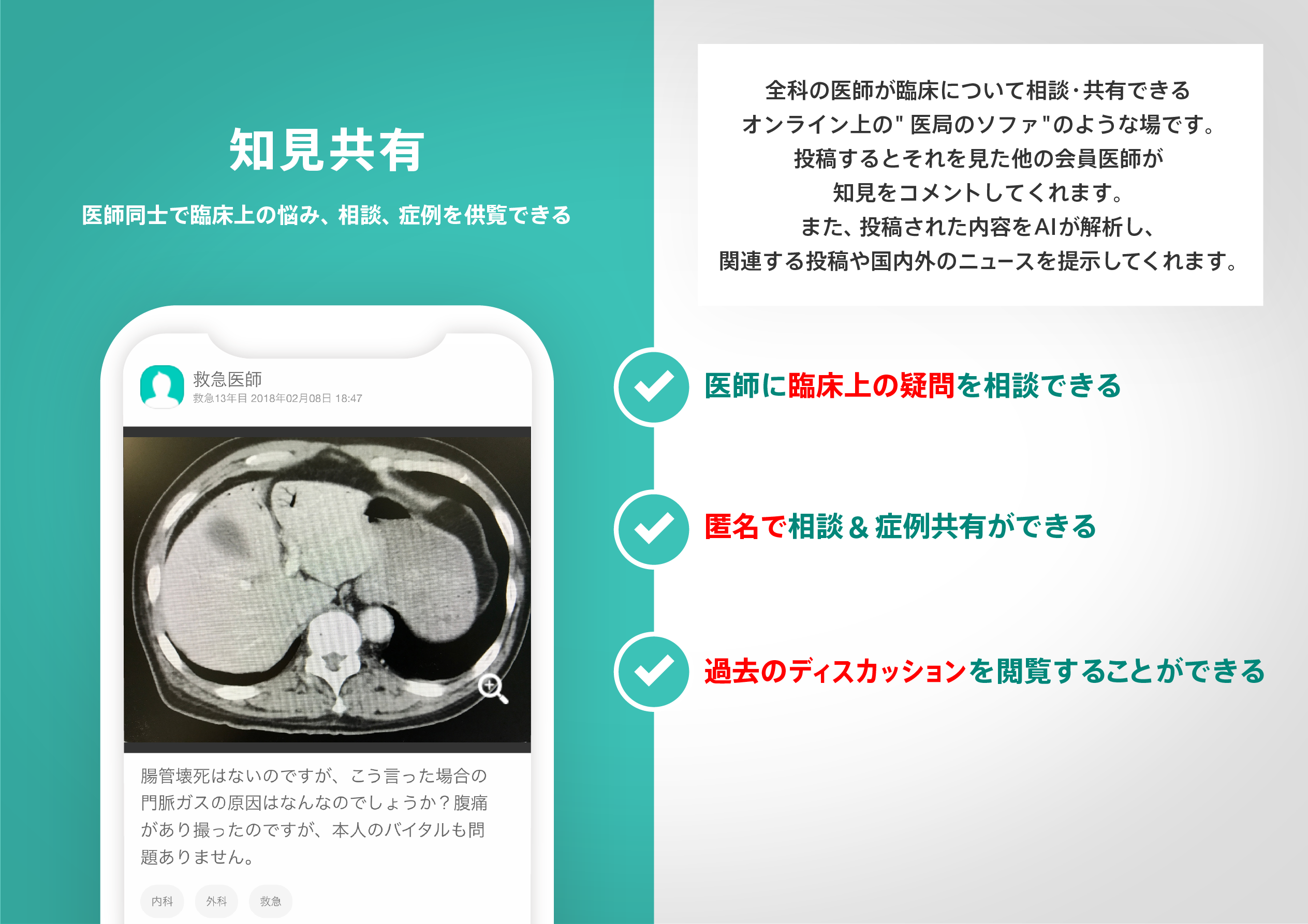
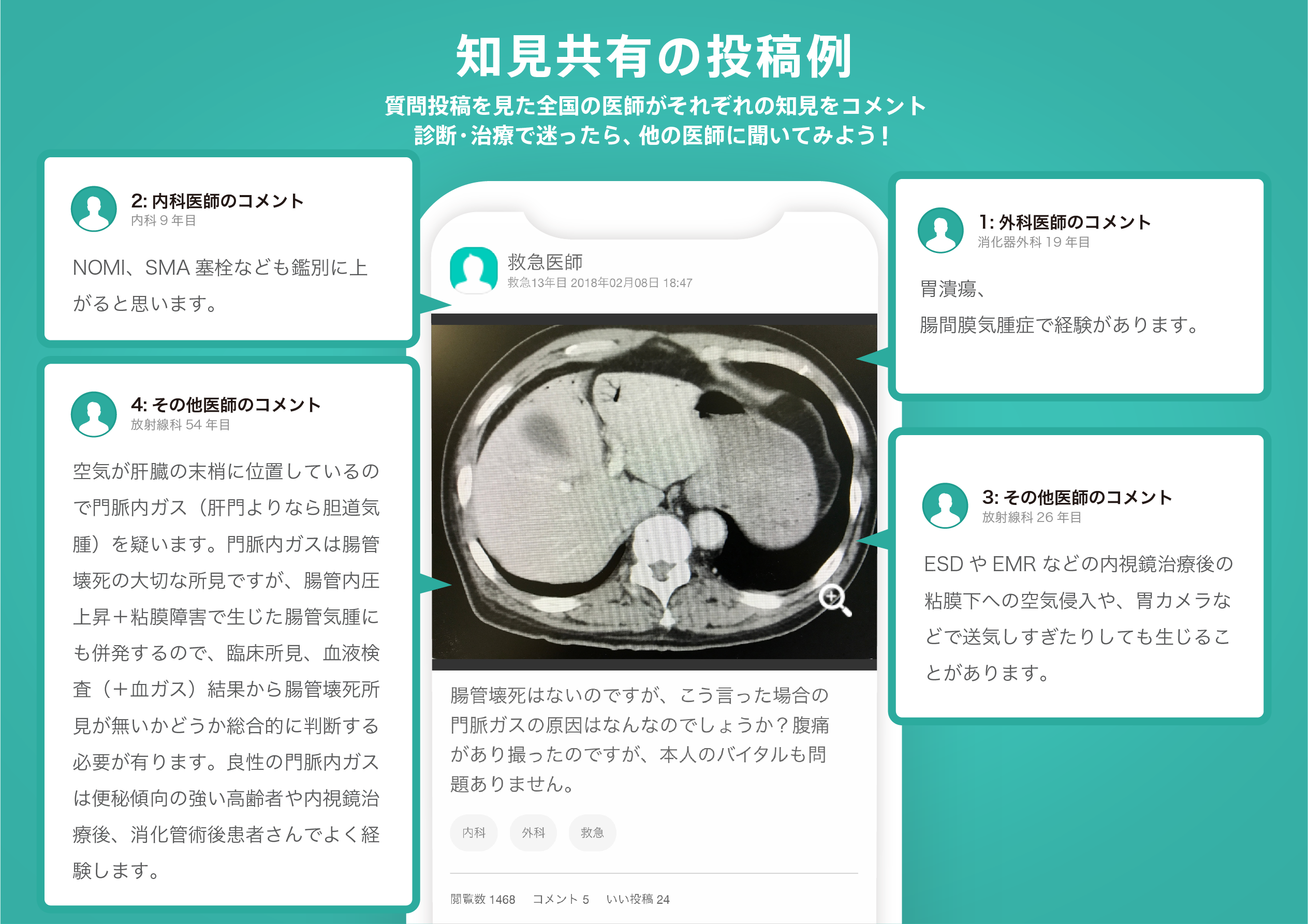
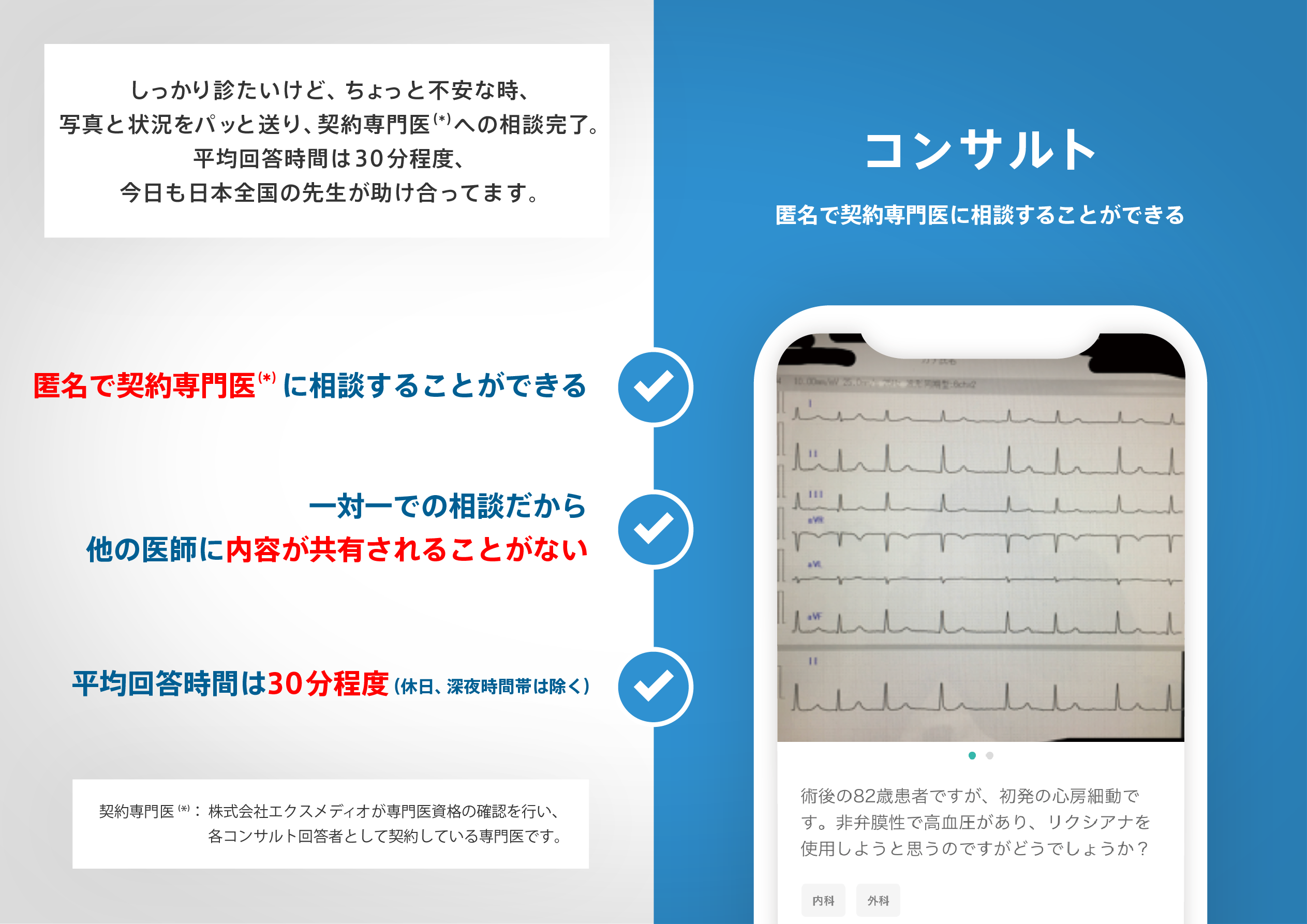
医師のための臨床サポートサービス
ヒポクラ x マイナビのご紹介

無料会員登録していただくと、さらに便利で効率的な検索が可能になります。