著名医師による解説が無料で読めます
すると翻訳の精度が向上します
(AlxGa1-X)2O3/Ga2O3構造で構成される二重バッファー層を使用して、ミスト化学蒸気堆積を使用したサファイア基板上のSNドープα-Ga2O3エピタキシャル薄膜を成長させました。二重バッファー層の挿入により、基質によって生成された脱臼をブロックすることにより、上部成長したSNドープα-Ga2O3薄膜の結晶品質が改善されました。700〜800°Cの位相遷移温度で、二重バッファー層に対して急速な熱アニーリングを実施しました。κとβ相のわずかな混合により、局所的な外側成長を通じて成長したSN-GA2O3薄膜の結晶性がさらに改善されました。SN-GA2O3薄膜の電子移動度も、滑らかな界面とAlの拡散により大幅に改善されました。したがって、ダブルバッファー層を使用した急速な熱アニーリングは、より短い処理時間内にGa2O3半導体デバイスの強力な電気特性を達成する上で有利であることが判明しました。
(AlxGa1-X)2O3/Ga2O3構造で構成される二重バッファー層を使用して、ミスト化学蒸気堆積を使用したサファイア基板上のSNドープα-Ga2O3エピタキシャル薄膜を成長させました。二重バッファー層の挿入により、基質によって生成された脱臼をブロックすることにより、上部成長したSNドープα-Ga2O3薄膜の結晶品質が改善されました。700〜800°Cの位相遷移温度で、二重バッファー層に対して急速な熱アニーリングを実施しました。κとβ相のわずかな混合により、局所的な外側成長を通じて成長したSN-GA2O3薄膜の結晶性がさらに改善されました。SN-GA2O3薄膜の電子移動度も、滑らかな界面とAlの拡散により大幅に改善されました。したがって、ダブルバッファー層を使用した急速な熱アニーリングは、より短い処理時間内にGa2O3半導体デバイスの強力な電気特性を達成する上で有利であることが判明しました。
Double buffer layers composed of (AlxGa1-x)2O3/Ga2O3 structures were employed to grow a Sn-doped α-Ga2O3 epitaxial thin film on a sapphire substrate using mist chemical vapor deposition. The insertion of double buffer layers improved the crystal quality of the upper-grown Sn-doped α-Ga2O3 thin films by blocking dislocation generated by the substrates. Rapid thermal annealing was conducted for the double buffer layers at phase transition temperatures of 700-800 °C. The slight mixing of κ and β phases further improved the crystallinity of the grown Sn-Ga2O3 thin film through local lateral overgrowth. The electron mobility of the Sn-Ga2O3 thin films was also significantly improved due to the smoothened interface and the diffusion of Al. Therefore, rapid thermal annealing with the double buffer layer proved advantageous in achieving strong electrical properties for Ga2O3 semiconductor devices within a shorter processing time.
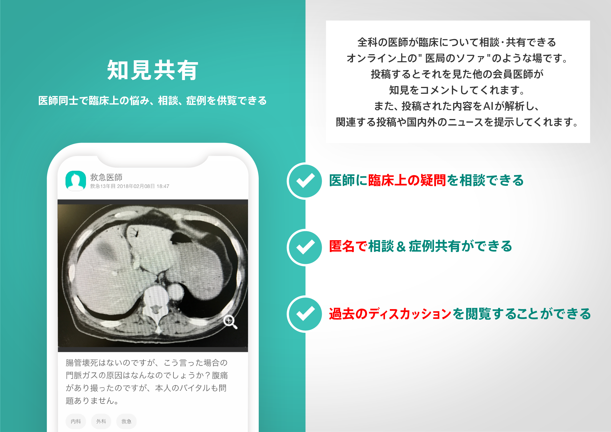
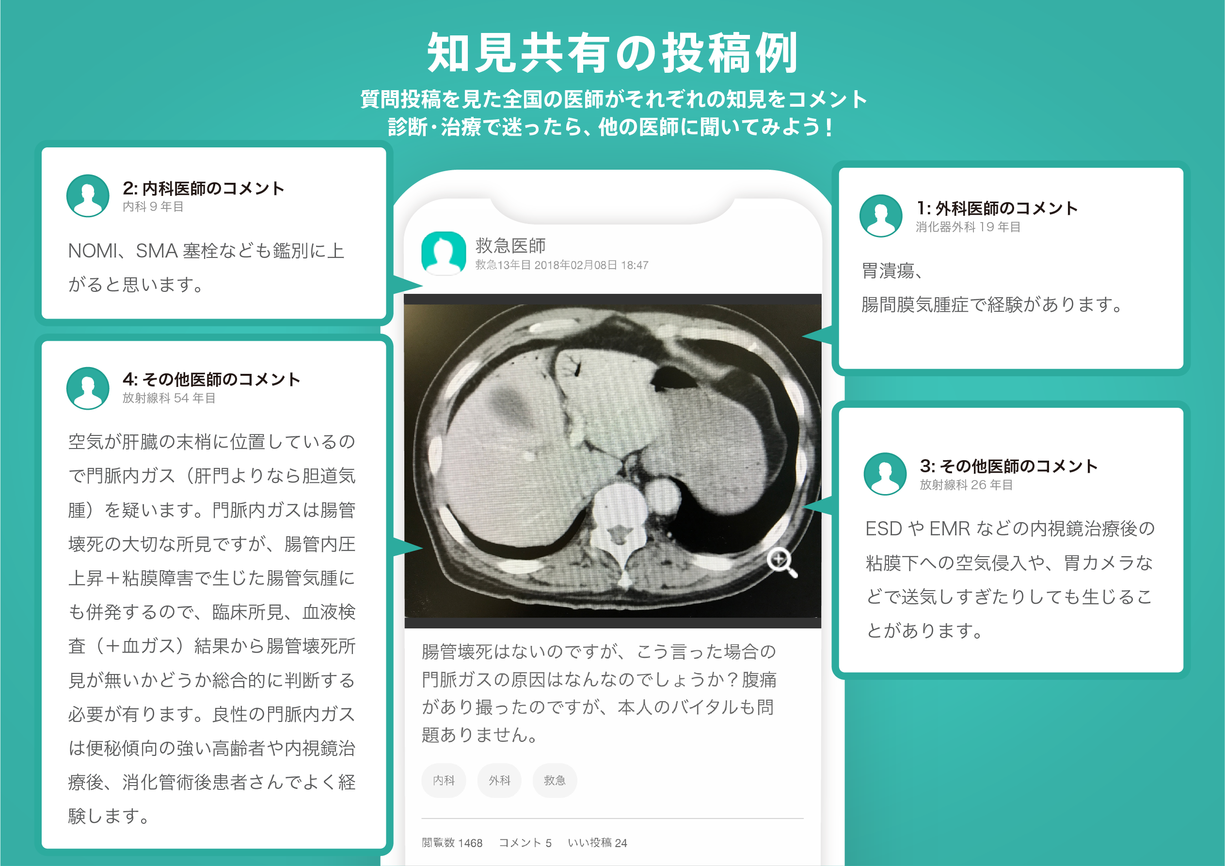
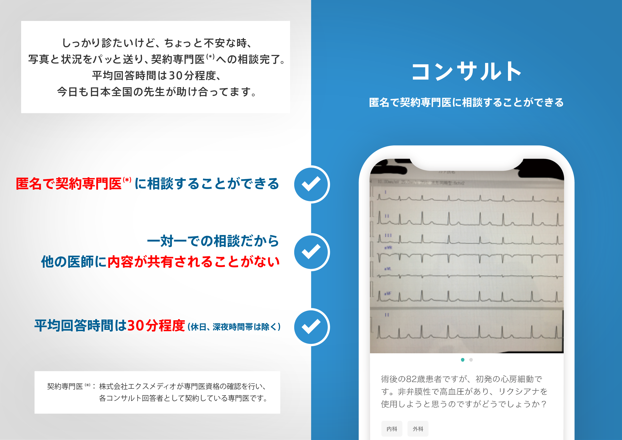
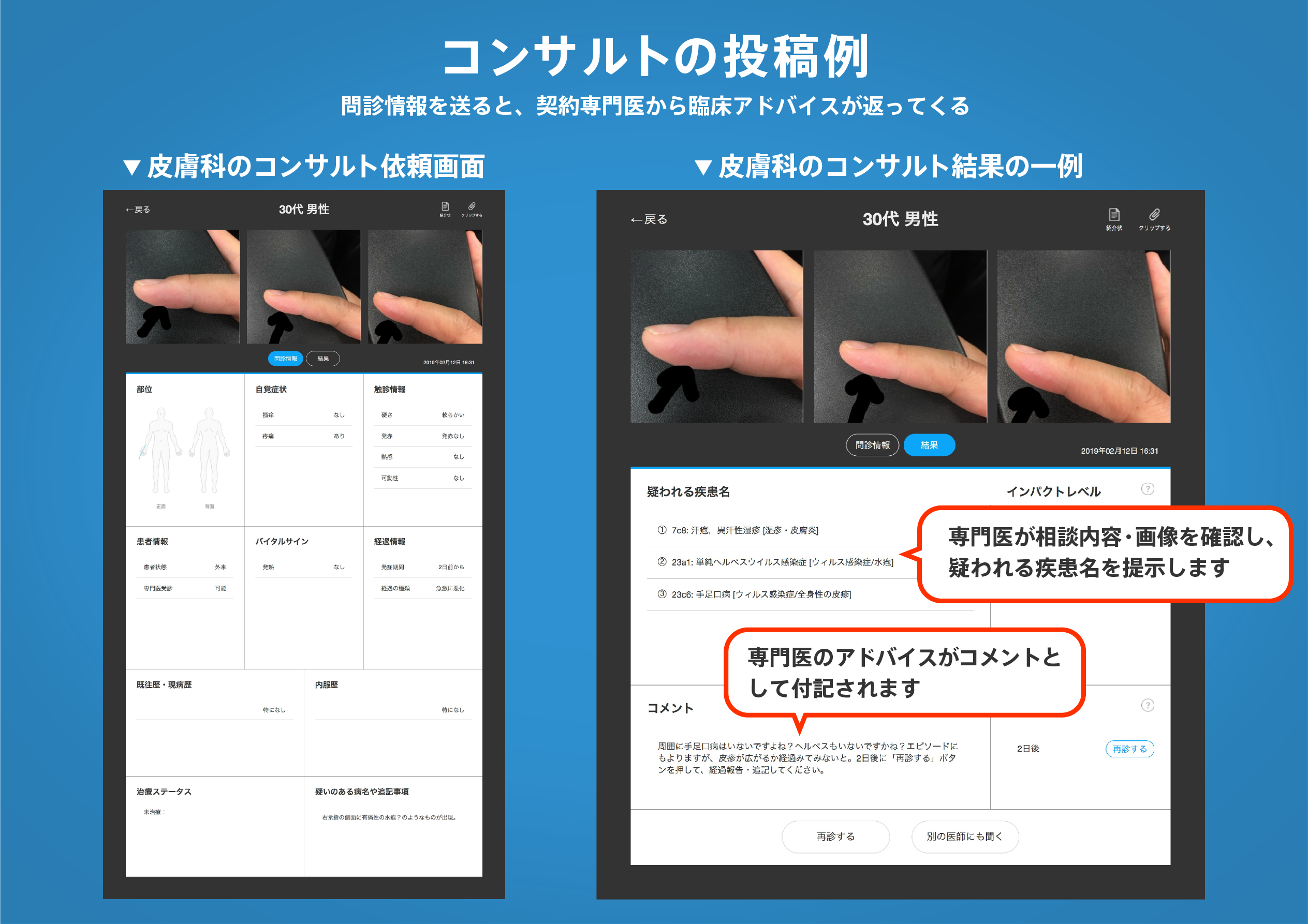
医師のための臨床サポートサービス
ヒポクラ x マイナビのご紹介


無料会員登録していただくと、さらに便利で効率的な検索が可能になります。