著名医師による解説が無料で読めます
すると翻訳の精度が向上します
領域選択的原子層堆積(AS-ALD)TiO2のプロセスおよびsinのプロセス成長領域vs SiO2は、最先端の300 mm半導体ウェーハの製造によって作成されたパターンで非row波領域として実証されています。プロセスは、sin在来酸化物を除去し、Sio2表面をフッ素化種で並べる二重の役割を持つin situ CF4/N2プラズマエッチングステップで構成されているため、後者の表面の反応性が低下します。さらに、(ジメチルアミノ)トリメチルシランは、選択性をさらに高めるために小分子阻害剤(SMI)として使用されました。堆積プロセスを断続的なCF4/N2プラズマベースのバックエッチングステップと組み合わせるときに、実質的に完全な選択性が得られました。〜8および〜5 nmのアプリケーション互換厚さは、TiO2および血漿ALDの熱ALDについて得られました。
領域選択的原子層堆積(AS-ALD)TiO2のプロセスおよびsinのプロセス成長領域vs SiO2は、最先端の300 mm半導体ウェーハの製造によって作成されたパターンで非row波領域として実証されています。プロセスは、sin在来酸化物を除去し、Sio2表面をフッ素化種で並べる二重の役割を持つin situ CF4/N2プラズマエッチングステップで構成されているため、後者の表面の反応性が低下します。さらに、(ジメチルアミノ)トリメチルシランは、選択性をさらに高めるために小分子阻害剤(SMI)として使用されました。堆積プロセスを断続的なCF4/N2プラズマベースのバックエッチングステップと組み合わせるときに、実質的に完全な選択性が得られました。〜8および〜5 nmのアプリケーション互換厚さは、TiO2および血漿ALDの熱ALDについて得られました。
Area-selective atomic layer deposition (AS-ALD) processes for TiO2 and TiON on SiN as the growth area vs SiO2 as the nongrowth area are demonstrated on patterns created by state-of-the-art 300 mm semiconductor wafer fabrication. The processes consist of an in situ CF4/N2 plasma etching step that has the dual role of removing the SiN native oxide and passivating the SiO2 surface with fluorinated species, thus rendering the latter surface less reactive toward titanium tetrachloride (TiCl4) precursor. Additionally, (dimethylamino)trimethylsilane was employed as a small molecule inhibitor (SMI) to further enhance the selectivity. Virtually perfect selectivity was obtained when combining the deposition process with intermittent CF4/N2 plasma-based back-etching steps, as demonstrated by scanning and transmission electron microscopy inspections. Application-compatible thicknesses of ∼8 and ∼5 nm were obtained for thermal ALD of TiO2 and plasma ALD of TiON.
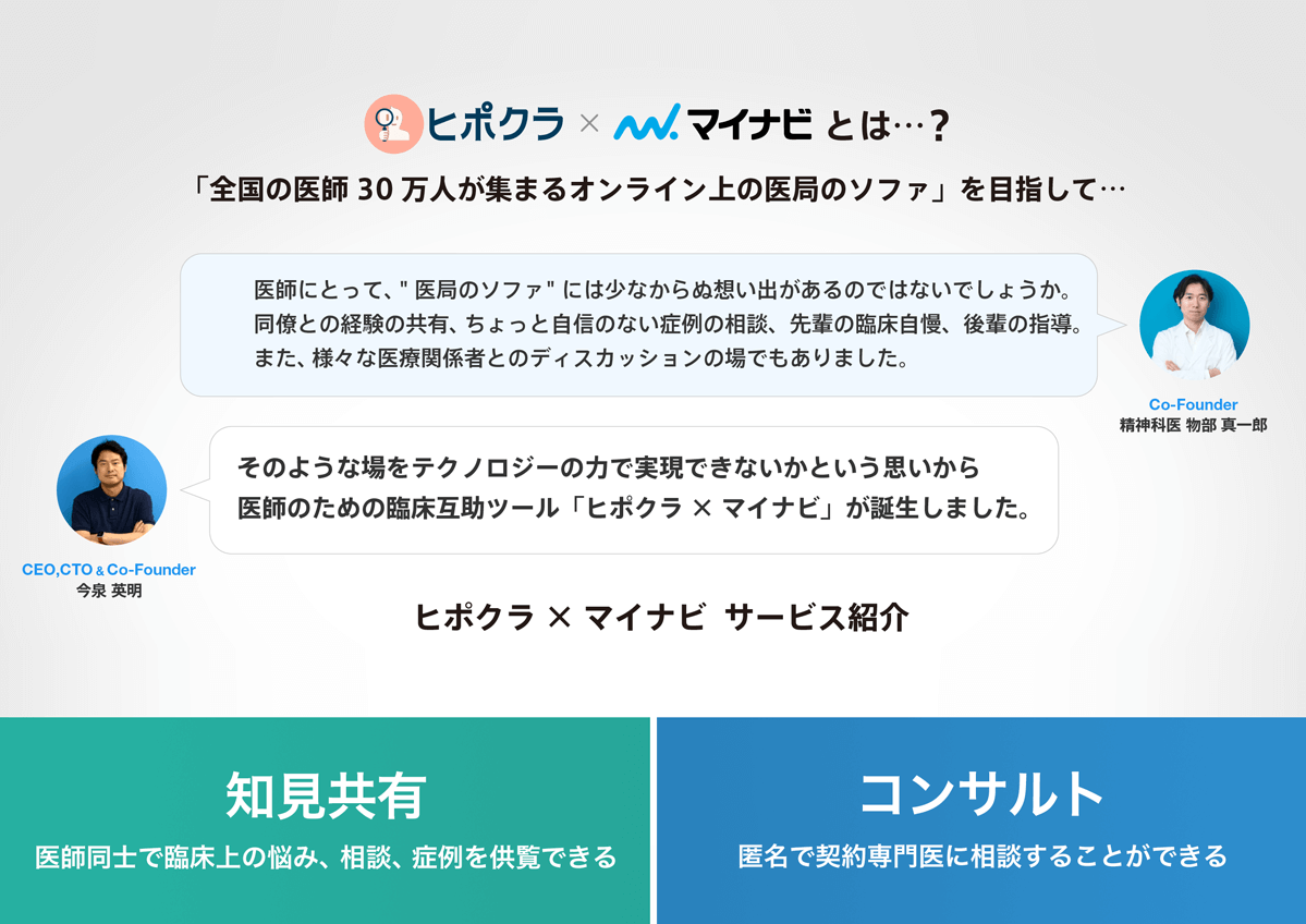
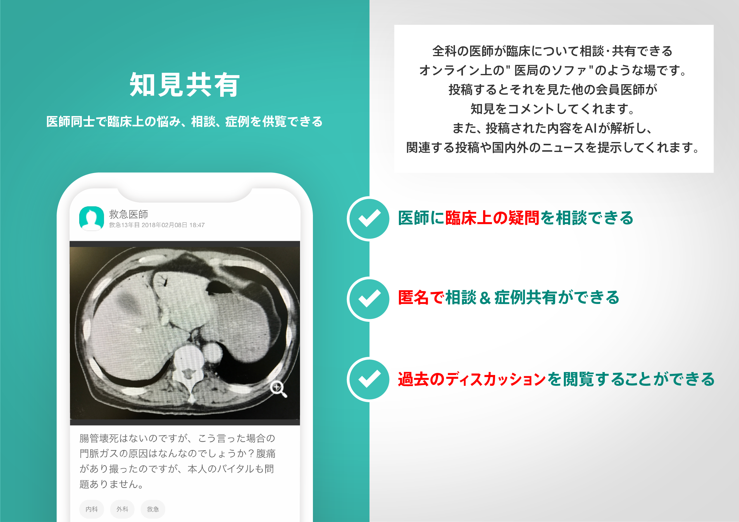
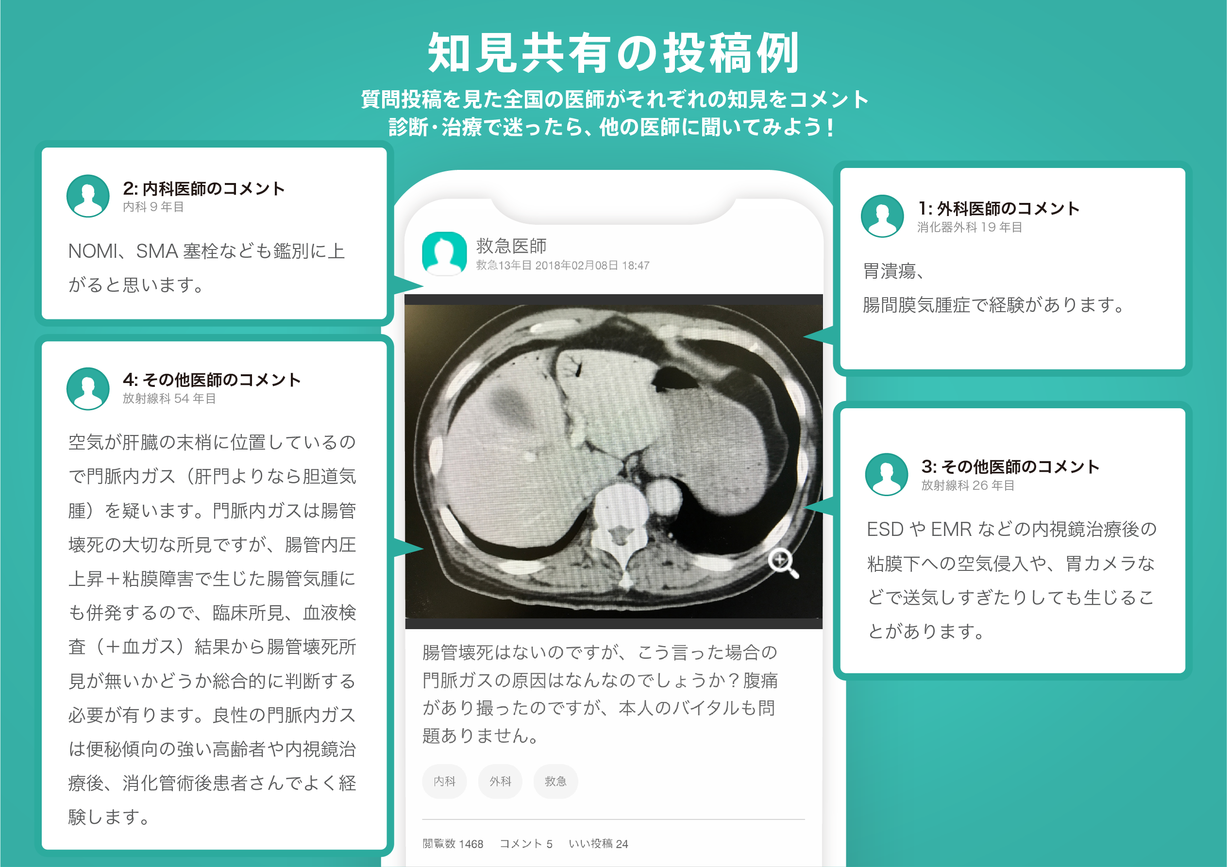
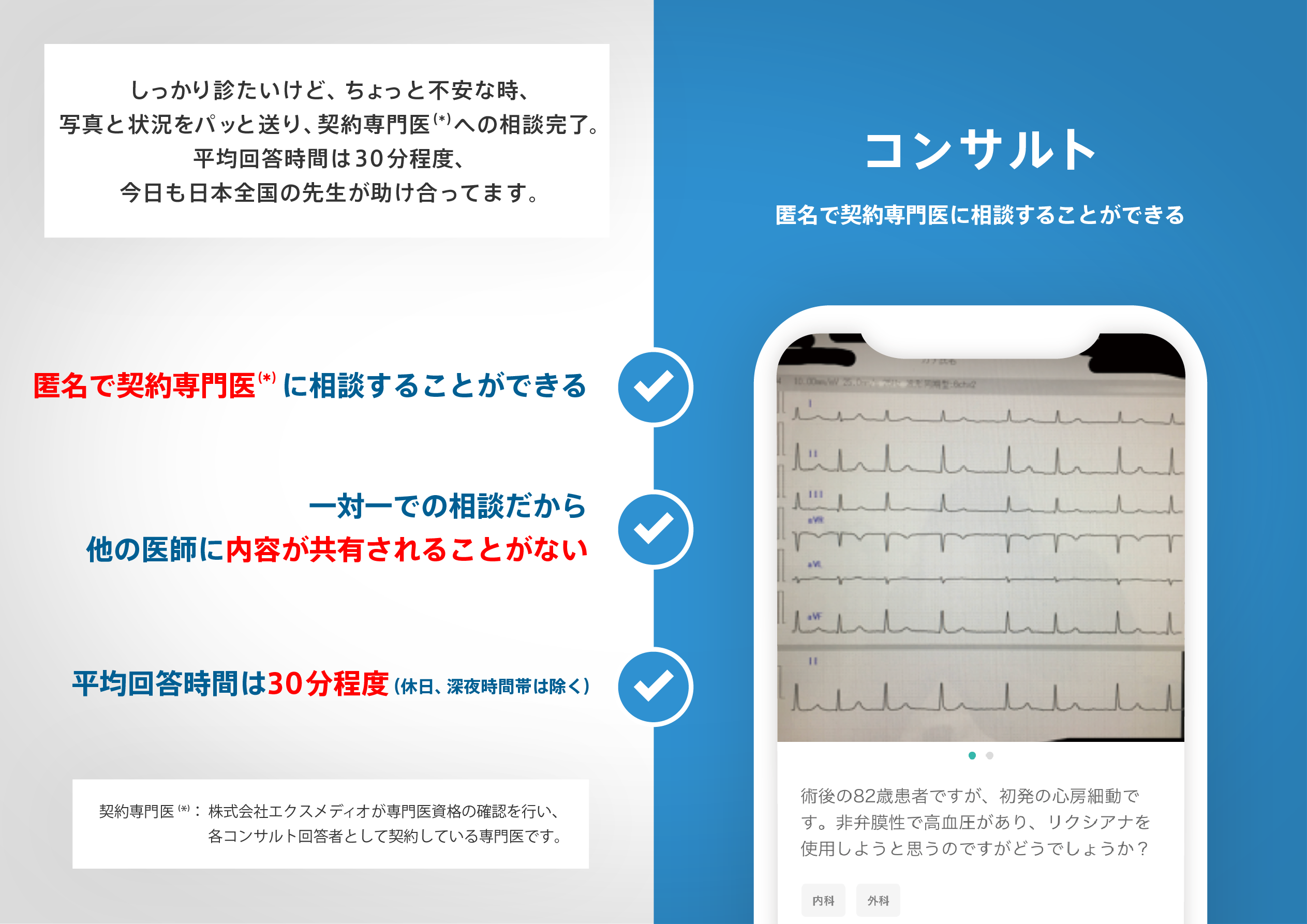
医師のための臨床サポートサービス
ヒポクラ x マイナビのご紹介

無料会員登録していただくと、さらに便利で効率的な検索が可能になります。